Voltage References from Diode to Band Gap: Part 3 – Band Gap References
So far in this blog series, we’ve learned when and why to use voltage references and a few techniques for generating these references, including the trade-offs of each technique. Here, we will learn how to use the band gap technique to generate high precision reference voltages. This method offers the best stability, precision, silicon size and cost versus the previous ways, but it is also more complex. However, when it comes to integrated circuits (ICs), band gap voltage references can be the easiest to implement. Let’s take a brief look at the physics to understand why.
What is Band Gap, and How Does it Relate to Semiconductors?
The concept of band gap comes from atomic physics. Electrons in the external layer (valence) are weakly tied to the atom and can become free if some energy is given to them. This energy can be light, radiation, vibration, or heat. The electrons become “free” by passing from the valence to the conduction band.
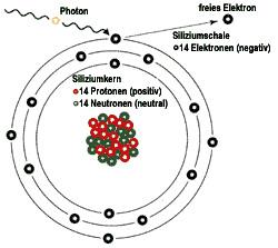
Atomic representation of energy triggering the release of valence electrons into the conduction band.
Band gap describes the amount of energy required for a valence electron to jump to the conduction band. Metals have no gap at normal temperatures, making them natural conductors, while isolators have a large gap even at high temperatures. Some elements are in between. Germanium, Silicon, and Gallium-Arsenide are called semi-conductors because they have a thin band gap. In Silicon, for example, the energy required to push a valence electron into the conduction band is close to 1.1 eV at room temperature (300°K).
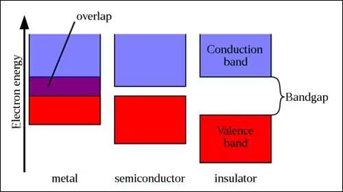
Band gap comparison for metals, semiconductors, and insulators
The relationship between energy and the band gap reference voltage is complex. The energy requirements are influenced by the atom, temperature, and dopant in the semiconductor layers. Those who are willing to put in the work, however, will be rewarded with tens of PPM of accuracy.
Band Gap Reference Principle
As we previously observed, a direct biased PN junction can be combined with a Zener voltage (above 6 volts) to balance out the components’ opposite temperature coefficients (tempco). In the band gap technique, the same principle is used by putting in series two voltage sources with opposite tempco. In this case, however, only transistors are used, no Zener. The two sources are called PTAT (positive vs T) and CTAT (complement vs T).
PTAT Construction: Using the Voltage Difference of Two PN Junctions
All forward bias junctions (diodes, BJTs) are known to have CTAT behavior of -1.8mV/°K. To create a band gap reference principle, a PTAT element must be fabricated with an inverse behavior of +1.8mV/°K and placed in series with the CTAT. For example, if one uses only a CTAT in situations with very diversified temperature (let's say -40°C and +125°C), the CTAT voltage can have an imprecision of greater than 300mV (= -1.8mV * (125-(-40)). A compensation trick is required: that’s a PTAT. So how do we achieve this target PTAT value?
Taken individually, each PN junction exhibits a CTAT behavior. But, if you subtract one from the other, you obtain a voltage that can be a PTAT! It all depends on the current imbalance between them. The simple answer is: We achieve our target PTAT value by differentiating the base-emitter voltages of the two bipolar transistors used to produce our CTAT, VBE1 – VBE2, versus T. As a reminder, VBE is the base-emitter voltage in a bipolar transistor initially forward biased and presenting 0.5 to 0.8 volt. Mathematically, this can be represented as follows:
(k/q)*Ln(I1/I2) * T = 86uV * Ln (I1/I2) * T = +k * T with k = 86uV * Ln (I1/I2).
However, reality is rarely as simple as the pure equation. Look closely and perhaps you’ll begin to see the problem.
To realize a value of k around +1.8mV/°K, Ln(I1/I2) must be around 21. That means I1 must be thousands or millions of times larger than I2! This result isn’t practical. The ratio is too big to use in any meaningful way. A ratio of 3 to 5, by comparison, would give us an Ln(I1/I2) value that is close to but greater than 1. That’s a number we can use! So how do we get there?
Adjusting Your Voltage Reference with Amplification
Amplifying the original PTAT can help keep the I1/I2 ratio more modest. To achieve this in our current example, we’ll need an amplifier of 21X in front of VBE1-VBE2 to compensate for the slope of -1.8mV/°K. That’s assuming ambient temperature and an Ln(I1/I2) close to 1. By applying an amplification factor of 1800 µV/86µV = 21 to the original PTAT, we get 0.7V + 0.543V = 1.243V as a stable reference voltage with a tempco factor very close to 0.
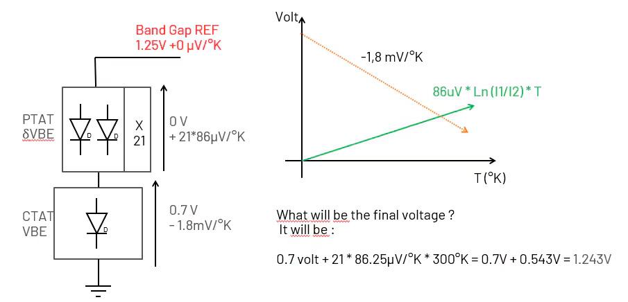
Charting the final voltage after applying 21x amplification
Practical Application: Building the CTAT + PTAT*21
The trick to generating delta VBE (without the need to put a subtractor function) is to apply a first VBE to a second VBE in which a resistor has been inserted in series with the emitter. The resistor (here R3) collects the VBE difference. The current in R3 then acts as a PTAT, and so does the current in its collector. If one inserts a resistor in the second collector, the latter will also exhibit PTAT behavior.
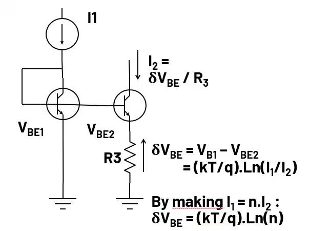
Combining circuit elements to achieve PTAT behavior
With our CTAT and PTAT in place, we can now build our band gap voltage reference according to the diagram in Figure 7, knowing that:
- The CTAT is provided by the T3 base-emitter.
- The PTAT is generated by one or more of the following:
- Delta VBE between T1 and T2
- Delta VBE on R2
- T2 emitter and collector currents exhibiting PTAT behavior
- Voltage on R3
- 1.25 voltage on OPAMP+, amplified by (1+R5/R6)
- A 21x amplifier compensates for the -1.8mV/°K of the CTAT
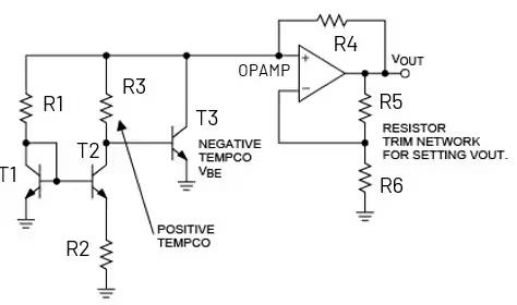
Complete circuit diagram for building a band gap voltage reference
Summary
In this post, we learned how to build a band gap voltage reference by cascading two sources with opposite tempco: The CTAT from a forward biased PN junction and a PTAT as the difference between two CTAT, amplified 21 times. The band gap voltage reference method delivers greater precision and stability than other methods we’ve studied, but the cost of this improvement is complexity. For those Engineering Minds who are up to the challenge, you'll enjoy accuracy improvements in the range of tens of PPM.

