Understanding Memory Controllers: Key to Optimizing Computer Performance
The memory controller is a vital component of the computer system that oversees the memory and facilitates data exchange between the memory and the CPU. The memory controller determines the maximum memory capacity that the computer system can utilize, the number of memory banks, memory type and speed, memory particle data depth and data width, and other crucial parameters. The memory controller determines the memory performance of the computer system, which has a significant impact on the overall performance of the computer system.
A physical address is used by the CPU to access information stored in memory. However, the CPU does not directly handle this process; instead, it delegates this task to the memory controller chip, also known as the MCC.
The Memory Controller Chip
Catalog
1 Classification of the memory controller
2 Working principle of the memory controller
3 Advantage and disadvantage
4 To sum up
1 Classification of Memory Controller
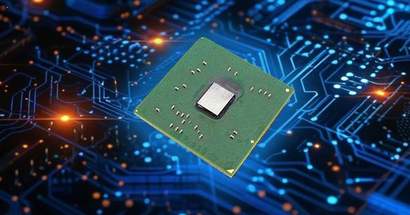
With the development of computer technology, memory controllers are divided into traditional and integrated types.
memory controller
1)Traditional Memory Controller
The memory controller of a traditional computer system is located in the north bridge chip of the motherboard chipset. To exchange data with the memory, the CPU must go through the five steps of "CPU-North Bridge-Memory-North Bridge-CPU". In this mode, the data passes through multi-level transmission, the data delay is obviously relatively large, which affects the overall performance of the computer system.
2) Integrated memory controller
Integrated memory controller means to build a memory controller on the basis of the CPU. Let us talk about how the system works without a memory controller. The 26 data A~Z must be transferred to the CPU. The CPU gives an instruction to the Northbridge. Since the memory controller is integrated on the northbridge, it is said to pass through the northbridge. The memory receives the instruction through the memory controller. This instruction transfers the A~Z data of unit b in the memory to the CPU, and the memory starts to fetch the data at this time, which is usually referred to as addressing. When the memory finds this data, and each of these 26 data is 500MB, the sum of all the data is about 12GB. Assuming that the memory is a dual-channel R2 800, the data transfer rate is 800MHZ multiplied by 128BIT divided by 8 bits per byte = 12GB per second. Through analysis, it is assumed that it takes only one second to transfer the data to the CPU. The data is transferred to the North Bridge in only one second. The memory controller is located in the North Bridge.
How is the data in the North Bridge transferred to the CPU? It must be through the FSB front-side bus. Assuming the FSB frequency is 800MHZ, then the data transfer rate is multiplied by 64BIT divided by 8 bits per second = 6.4GB per second. It takes 2 seconds from the North Bridge to the CPU, so the total time for data transfer to the CPU is 3 seconds.
Next, let's look at the CPU's integrated memory controller system. How does it work? After the data is transferred from the memory to the controller, it also takes 1 second. The difference is that this time does not need to go through the slow front-side bus, the CPU reads the data directly from the memory controller because the memory controller is at the door of the CPU. For example, if an item is at your door, anyone can take it directly. The CPU of the integrated memory controller reads 12 GB of data. The time is 1 second, so the calculation time is greatly reduced, and the performance of the CPU is also fully utilized.
Finally, to summarize, when the CPU has no memory controller, the data transfer is the memory controller --- Northbridge - CPU; when there is a memory controller, the data transfer is from the memory controller - CPU.
2 Working Principle of Memory Controller
1)Memory frequency
Like the CPU, the memory has its own operating frequency. The frequency is measured in MHz. The higher the memory frequency, the faster the memory can operate. The memory's base frequency determines the maximum frequency at which the memory can operate normally. The most common memory types are DDR3 and DDR4. As a replacement for DDR2, the frequency of DDR3 memory has reached 1600MHz, while the frequency of DDR4 memory is 2133MHz.
2)Memory Capacity
Memory capacity is not only a factor that affects the price of memory, but also a factor that affects the performance of the whole system. In the past Windows XP platform, 512M of memory was still the mainstream, and 1GB was already a large capacity. 64-bit systems began to spread, Windows Vista, Windows 7 and Windows 10 were used by more and more people. Without about 2GB of memory, smooth operation may not be guaranteed. The capacity of a single memory is 1GB, 2GB, 4GB. The highest has reached 8GB and 16GB.
3)Operating voltage
The voltage required by memory for normal operation is different, but each memory has its own specifications. Exceeding its specifications can easily cause memory damage. The operating voltage of DDR2 memory is generally around 1.8V, while DDR3 memory is around 1.5V or 1.35V. In order to overclock, the memory needs to operate at a higher voltage than the standard. For each brand and model of memory, it depends on the manufacturer. As long as it is within the allowable range, a slight increase in memory voltage is conducive to memory overclocking, but at the same time, the heat generation increases greatly, so there is a risk of hardware damage.
4)Timing Parameters
Memory Controller Parameters
tCL: CAS Latency Control(tCL)
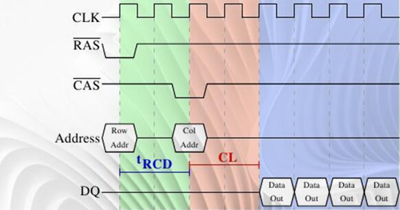
Generally, when we look up the timing parameters of the memory, such as "8-8-8-24". The corresponding parameters of the above digital sequences are "CL-tRCD-tRP-tRAS". The first "8" is the first parameter, the CL parameter.
CAS Latency Control (also referred to as tCL, CL, CAS Latency Time, CAS Timing Delay). CAS controls the time between receiving an instruction and executing it. Since CAS mainly controls the hexadecimal address or column address in the memory matrix, it is the most important parameter and should be set as low as possible for stability.
Memory is addressed by rows and columns. When the request is triggered, it is initially tRAS (Active to Precharge Delay). After precharge, the memory actually starts to initialize RAS. Once tRAS is activated, RAS (Row Address Strobe) begins addressing the required data. First the row address is addressed, then tRCD is initialized, the cycle ends, and then the exact hexadecimal address of the required data is accessed via CAS. The time from the start of CAS to the end of CAS is the CAS delay. Thus, CAS is the last step in finding data, and it is also the most important of the memory parameters.
This parameter controls how many clock cycles the memory waits after receiving a data read instruction before actually executing the instruction. At the same time, this parameter also determines the number of clock cycles required to complete the first part of the transfer in a memory burst transfer. The smaller the parameter, the faster the memory speed. Note that some of the memory may not run at low latency and data may be lost. And increasing the latency can make the memory run at a higher frequency, so if you need to overclock the memory, you should try to increase the CAS latency.
This parameter has the biggest impact on memory performance. Under the premise of ensuring system stability, the lower the CAS value, the faster the memory reads and writes.
tRCD: RAS to CAS delay
This value is the second parameter in the memory timing parameters of "8-8-8-24", i.e. the second "8". RAS to CAS Delay (also referred to as tRCD, RAS to CAS Delay, Active to CMD) means "Row Addressing to Column Addressing Delay Time". The smaller the value, the better the performance. When reading, writing, or refreshing memory, a delay clock cycle must be inserted between these two pulse signals. This is the second parameter in the JEDEC specification. Reducing this delay can improve system performance. If the overclocking performance of your memory is not good, you can set this value to the default value of the memory or try to increase the tRCD value.
tRP: Row Precharge Timing (tRP)
This value is the third parameter in the memory timing parameters of "8-8-8-24", i.e. the third "8". Row Precharge Timing (also referred to as tRP, RAS Precharge, Precharge to active) means "memory row address controller precharge time". The smaller the precharge parameter, the faster the memory read and write speed. tRP is used to set the charge time required by RAS before another row can be activated.
tRAS: Min RAS Active Timing
This value is the last parameter in the memory timing parameters of "8-8-8-24", i.e. "24". Min RAS Active Time (also referred to as tRAS, Active to Precharge Delay, Row Active Time, Precharge Wait State, Row Active Delay, Row Precharge Delay, RAS Active Time), which means "the shortest time from the effective memory row to precharge". The setting of this parameter must be determined according to the specific situation, generally we'd better set it between 24~30.
If the tRAS cycle is too long, the system will lose performance due to unnecessary waiting. Reducing the tRAS cycle will cause the active line address to enter the inactive state earlier. If the tRAS period is too short, the burst transmission of data may not be completed due to lack of time, which may result in data loss or corruption. This value is typically set to CAS latency + tRCD + 2 clock cycles.
3 Advantages and Disadvantages
1)Advantage
The advantage of integrating the memory controller into the CPU is that it can effectively control the memory controller to operate at the same frequency as the CPU core, and since the data exchange between the memory and the CPU does not need to go through the Northbridge, it can effectively reduce the transmission delay. For example, this is like moving the goods warehouse directly next to the processing workshop, which greatly reduces the time required to transport raw materials and finished products between the goods warehouse and the processing workshop. As a result, the overall performance of the system was also improved.
Reducing the load on the North Bridge chip. Because the amount of data exchanged between the CPU and memory accounts for a large proportion of the total data exchanged by the computer. The workload of the North Bridge chip is greatly reduced after integration, and it provides more efficient support for the data exchange channel of SATA, PCI-E, etc.
2)Disadvantage
The main disadvantage of the integrated memory controller inside the CPU is that it has poor memory adaptability and flexibility. It can only use certain types of memory, and there are restrictions on the capacity and speed of the memory. It is necessary to update the CPU's internal integrated memory controller to support new types of memory, which means a new CPU must be replaced. For example, AMD's K8 series CPU can only support DDR, not the faster DDR2. The traditional memory controller is in the northbridge chip of the motherboard chipset, so there is no such problem. You only need to replace the motherboard, and you can use different types of memory without replacing the motherboard, such as the Intel Pentium4 series CPU. If the motherboard does not support DDR2, you can use DDR2 as long as you replace it with a motherboard that supports DDR2. If you have a motherboard that supports both DDR and DDR2, you can use DDR2 directly without replacing the motherboard.
4 To summarize
Many applications have more complex read patterns (almost random, especially when cache hits are unpredictable) and do not use bandwidth efficiently. A typical application of this type is business processing software. Even with CPU features such as out-of-order execution, it is limited by memory latency. For example, the CPU must wait for the data required for the operation to be loaded from memory before it can execute the instructions. The memory latency of the current low-end system is about 120-150ns, and the CPU speed has reached more than 3GHz, a single memory request can waste 200-300 CPU cycles. Even if the cache hit rate is 99%, the CPU may spend 50% of the time waiting for the end of the memory request due to memory latency.
The memory controller of a traditional computer system is located in the Northbridge chip of the motherboard chipset. The CPU needs to exchange data with the memory through five steps of "CPU-Northbridge-Memory-Northbridge-CPU". In this mode, data is transferred through multiple levels, and the data delay is obviously relatively large, which affects the overall performance of the computer system. AMD's K8 series CPUs (including various processors with Socket 754/939/940 interfaces) integrate a memory controller. The data exchange process of CPU and memory is simplified to the three steps of "CPU-Memory-CPU", and two steps are eliminated. Compared with the traditional memory controller solution, the data delay is significantly lower, which helps to improve the overall performance of the computer system.


