Die-Attach Process Handles the Heat of GaN Transistors
As power demands increase for transistors in automotive, industrial, and renewable energy applications, traditional packaging methods struggle to dissipate waste heat efficiently. This limitation often requires downrating transistors’ performance to prevent overheating, which impedes advancements in high-power electronics. Current die attachment techniques face challenges such as thermal resistance and stress-induced failures, creating significant reliability concerns for industries where consistent performance is critical.
QPT’s qAttach process solves these challenges by introducing a novel die attachment method that significantly enhances heat transfer while reducing manufacturing stresses. This technology supports the increasing power and frequency demands of gallium nitride (GaN) transistors and paves the way for more reliable and efficient power electronics across various industries.
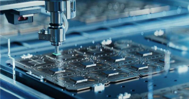
Die attach process. Image used courtesy of Adobe Stock
Conventional Heat Removal Challenges in Power Electronics
In traditional power electronics packaging, the die is attached to a substrate—typically aluminum nitride—using a sintering process. This method involves applying a sinter layer, usually 30 to 60 microns thick, to bond the die and substrate. However, this layer acts as a thermal barrier, impeding heat transfer from the die to the heat sink. Since heat dissipation is crucial for maintaining transistor performance and preventing overheating, this limitation forces designers to downrate the transistors, reducing their operational efficiency.
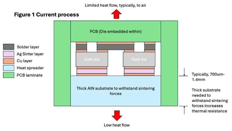
The conventional attachment process involving the sinter layer. Image used courtesy of QPT
Additionally, the sintering process requires significant pressure during manufacturing, which places mechanical stress on the die and substrate. These stresses, combined with the differing thermal expansion rates of the materials, can lead to delamination, a significant cause of failure in high-power packages. Thermal resistance, manufacturing complexity, and stress-induced reliability issues highlight the need for a more effective attachment process.
QPT’s qAttach Method
QPT’s qAttach process improves die attachment by replacing the thick sinter layer with an ultra-thin attachment layer, reducing the thermal barrier thickness to a micron fraction. This drastic reduction in thermal resistance allows heat to transfer more efficiently from the die to the substrate and heat sink, improving overall heat removal rates by up to 15 times.
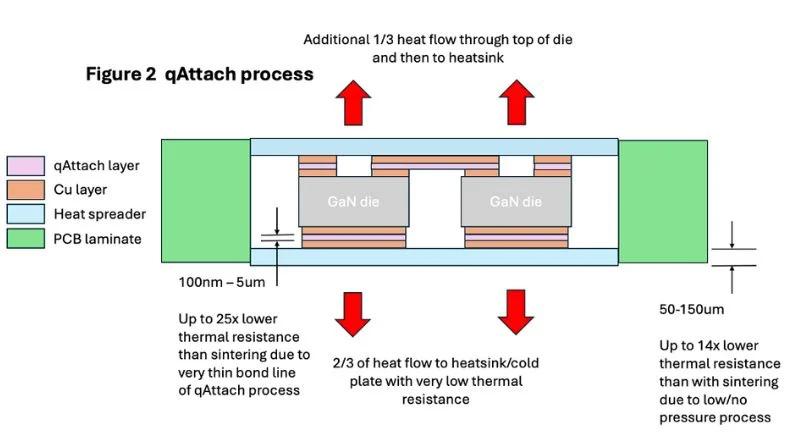
The qAttach process. Image used courtesy of QPT
Unlike conventional sintering's continuous sheet structure, the qAttach layer features a proprietary geometry to constrain expansion primarily in the Z-axis. This minimizes mechanical stress during thermal cycling and eliminates delamination risk. Additionally, qAttach enables heat dissipation from the top and bottom of the die, further enhancing cooling performance.
The manufacturing process for qAttach also requires less pressure than sintering, allowing for thinner substrates and reducing stress on the components. This innovation increases thermal efficiency and simplifies the manufacturing process.
Benefits of qAttach Technology
qAttach’s benefits extend beyond improved heat removal. Minimizing thermal resistance and manufacturing pressure enables GaN transistors to operate at higher power levels and frequencies without overheating, opening possibilities for GaN adoption in high-power applications. Finally, the thinner substrates enabled by qAttach also reduce material costs, contributing to more cost-effective manufacturing processes.
By overcoming the limitations of conventional die attachment methods, QPT’s qAttach technology delivers a universal solution to the growing challenges of waste heat removal in power electronics.