ISSCC: Sony Pushes Global Shutter to Commercial Cameras With Image Sensor
This week, the International Solid-State Circuits Conference (ISSCC) ushered global researchers to San Francisco, California, to show off their latest developments in the world of electronics.
At the conference, Sony Semiconductor introduced a new 25.2 MP full-frame global-shutter CMOS image sensor designed to alleviate common issues with traditional rolling shutter technology. While global shutter (GS) has been available for some time now, especially in the world of industrial or broadcast cameras, it has not yet matured enough to be commercially viable for consumer camera technologies. This could all change very soon, however, thanks to the latest developments from Sony.
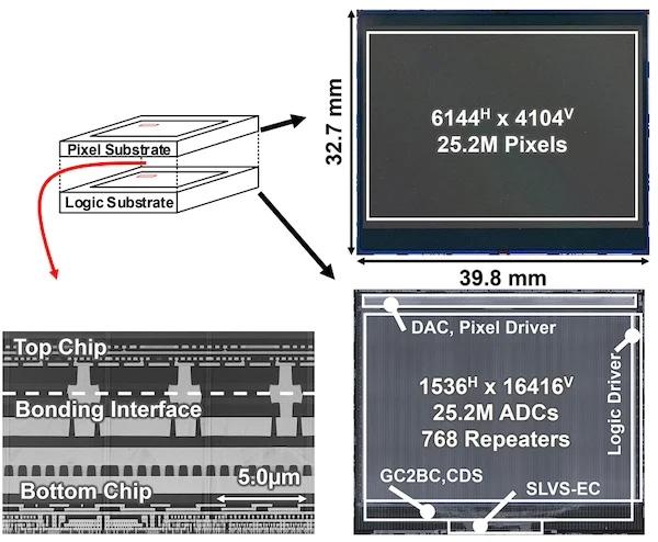
Sony’s new global shutter CMOS image sensor uses two stacked chips to read every pixel at once and improve the performance of cameras.
This could all change very soon, however, thanks to the latest developments from Sony, which has implemented its sensor in a 90-nm CMOS process.
Global Shutter for Better, Faster Cameras
Rolling shutter image sensors form an image by sampling and processing each row of pixels individually. If this process occurs fast enough, the sensor can take a good image of a static scene. Rolling shutters are typically easier to implement since they only require hardware for a single row of pixels and can share this hardware between all rows. If, however, an item in the frame is moving during this shutter, its position will change slightly between the times when each row is sampled, creating blurred or flickering images.
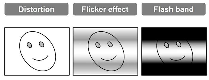
With rolling shutters, moving objects can be distorted as a result of the longer exposure time of the image sensor.
To combat this, GS sensors sample all pixels at the same time. This can greatly improve image quality but is more difficult to implement since the number of ADCs, comparators, and other hardware building blocks increases with the number of pixels instead of the number of rows. With advanced semiconductor designs, however, global shutters are quickly becoming a more viable option for professional and amateur photographers.
Vertically Integrating Logic and Imaging
The Sony GS image sensor stacks two independent chips with a Cu-Cu bonding mechanism. Each pixel in the top chip, when exposed to light, will output a current proportional to the amount of light incident on the photodiode. This current (as well as a reference) is passed to the logic chip, located underneath the pixel chip, through the Cu-Cu hybrid bonding approach.
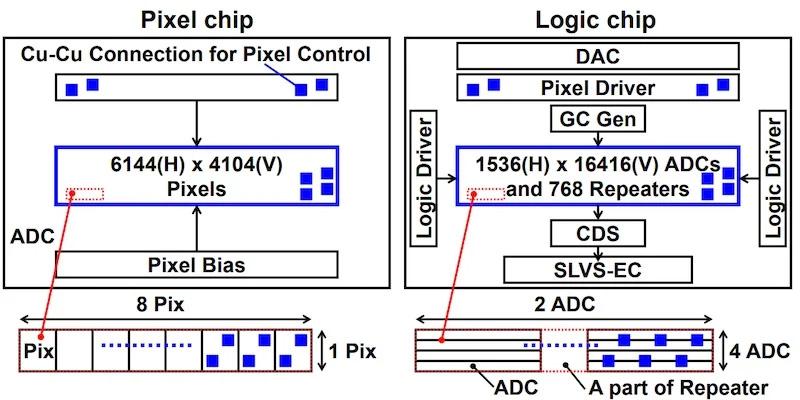
The block diagram of the Sony GS chip highlights how the pixel and logic chip can be directly bonded, providing sufficient processing hardware for GS imaging.
At the logic chip, the reference current converts to a voltage that can be digitized and used to provide a readout of the image. A key innovation of the chip is that each 8×1 group of pixels has an associated 4×2 array of ADCs immediately underneath them, making bonding and routing simpler and providing a high density of ADCs.
![]()
The block diagram of a single pixel and processing chain demonstrates how Sony was able to densely integrate the ADCs with good power efficiency and high speeds.
Some highlights of this chip are a maximum frame rate of 120 fps, an associated resolution of 25.2 MP (with 50.4 million Cu-Cu bonds), and a 2.66 e-rms random noise. In addition, the power consumption of the chip is very low, with a reported 1545 mW of consumption for the 25.2-MP design. In all, the Sony GS image sensor reports a FoM of 0.083, placing it well within striking distance of standard rolling shutter architectures and making it a more viable option for commercialization.
Making GS Image Sensors Mainstream
Sony’s new GS CMOS image sensor marks a step toward making GS image sensors more mainstream and accessible for designers and users alike. As the design matures, Sony intends to continue to improve power efficiency and frame rate to target even more applications.


