
Comprehensive Guide to Time Delay Circuits: From Timer Delay Circuits to Delay Pedals
In the field of digital circuit design, it is sometimes necessary to introduce a delay in the signal path. This can be achieved by introducing a delay in the signal itself, or by introducing a delay in another signal. A typical delay circuit is a string guide, and the delay time is the sum of the delays of each guide. Electronic delay circuits are used to create precise timing mechanisms for various applications, including safety and audio effects.
How to make a simple delay circuit
Catalog
1. Precise long delay circuit
2. RC delay circuit
3. 555 simple long delay circuit
4. Long-delay circuit consisting of two 555 time-based circuits
5. Monostable delay circuit with a single op-amp
6. Transistor delay circuit
It is common practice to use software components to achieve time delays, such as timers and similar tools. Today, we will discuss the methods for achieving timing with hardware, despite the inherent inaccuracy. Today, we will introduce six types of delay circuit working principles.
1. Precise Long Delay Circuit:
The circuit comprises a CD4060 as the timer's time base circuit. The timing time base pulse generated by the circuit is divided by the internal frequency divider, after which the time base signal is output. The timing control time is obtained by dividing the frequency through the external frequency divider circuit. This type of circuit can be used in applications requiring a time delay circuit breaker for safety applications and the delay pedal circuit for audio effects.
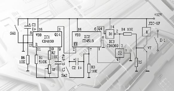
Precise Long Delay Circuit
Once the power is turned on, the time base oscillator begins to oscillate, generating the time base signal. The count division is initiated by IC2 of the divider. When counting to 10, Q4 outputs a high level. The high level is inverted by D1 to a low level, effectively cutting off the power supply to the controlled circuit.
Concurrently, the low level of D1 output is inverted to a high level by D2 and then added to the CP terminal of IC2, thus maintaining the high-level output of the output terminal.
Once the circuit has been energized to reset IC1 and IC2, the four outputs of IC2 will be at a low level. The low level of Q4 output is inverted to a high level by D1, which makes VT conductive through R4, and the relay is energized to absorb. This operational state is maintained throughout the power-on and power-off cycles.
2. RC Delay Circuit
The RC delay circuit is shown in the figure. The delay time of the circuit can be adjusted by the size of R or C. Due to the simplicity of the delay circuit, there is a disadvantage of short delay time and low accuracy. In instances where a longer and more precise delay is required, it is advisable to select a time relay. The RC delay circuit can also be adapted to function as a simple timer delay circuit, where the values of R and C determine the duration of the delay.
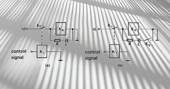
RC Delay Circuit
In automatic control, the relay delay circuit is sometimes used to ensure that the appropriate relay is engaged at the appropriate time within the predetermined period. Please find below a few examples of relay delay circuits.
The circuit shown in Fig. (A) is a cantoco-suction circuit. The circuit's on/off functionality is achieved through the charge and discharge of the RC, which is primarily utilized for short delays. In some instances, the relay is gradually released in accordance with the requirements of the control system. In such cases, the circuit shown in Fig. (B) can be utilized to facilitate the gradual release of the relay.
When the power is first turned on, since contact KK-l is in the normally open state, the RC delay circuit does not generate a delay during the suction process. Once the relay K is activated, its contact Kk-1 closes, allowing the release of relay KK to proceed at a slow rate. The time delay generated by the RC delay circuit can be calculated by using the following formula: R = 470K, C = 0.15uf time constant. This can be directly applied to R * C.
3. 555 simple long delay circuit
When the button SB is pressed, the 12V power supply is charged through the resistor RT to the capacitor CT, so that the potential of the pin 6 continues to increase. This circuit can be configured to create a 5-second delay circuit, which is a specific application of a timer delay circuit.
555 Simple Long Delay Circuit
The diode Vd1 on the pin 5 string causes the pin 5 potential to rise, resulting in a longer period than the general pickup (suspended or through small capacitance ground).
4. The long-delay circuit is comprised of two 555 time-based circuits.
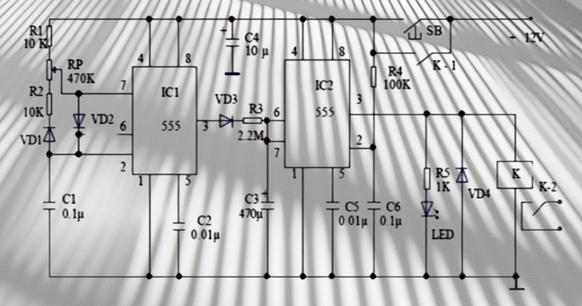
The IC1 555-time base circuit is connected as a self-excited multi-tuned oscillator with an adjustable duty cycle. Upon activation of the SB button, a 12V DC voltage is applied to the circuit. As the voltage of capacitor C6 cannot change abruptly, IC2 circuit pin 2 is low, indicating that the IC2 circuit is in a set state. The contacts K-1 and K-2 are closed, and the K-1 contact is closed to form a self-locking state. The K-2 contact is connected to the power device to control the power device.
The circuit comprises two 555 time-based circuits. At the same time, the IC1 555 time-based circuit begins to oscillate, resulting in the alternation of high and low outputs on the 3 pin. When the 3-pin output transitions to a high level, the capacitor C3 is charged by the diode VD3.
When pin 3 is output low, the diode VD3 is cut off, preventing the capacitor C3 from being charged. Consequently, capacitor C3 is only charged when pin 3 is at a high level. Please be aware that the charging time of capacitor C3 is quite lengthy.
Once the potential of capacitor C3 reaches 2/3 VDD, the IC2 555 time-base circuit is reset. When pin 3 outputs a low level, the relay K is de-energized, and the contacts K-1 and K-2 are disconnected, returning to the initial state and ready for the next timing cycle.
5. Monostable Delay Circuit with a Single Op-Amp:
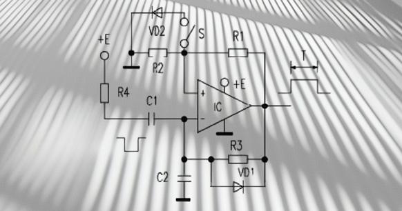
The monostable delay circuit employs a single operational amplifier and is a fundamental building block for more complex timing circuits, such as the analog delay circuit. In the normal state, the IC output remains low, maintaining a stable state. Upon the introduction of a negative pulse to the inverting terminal via C1, the potential of the inverting terminal is observed to be lower than that of the in-phase terminal. This results in a transition from a low to a high output, which is identified as an unstable state.
Monostable Delay Circuit with a Single Op-Amp
The high level is divided by R1 and R2 and then added to the in-phase terminal of IC, ensuring that the potential of the in-phase terminal is higher than that of the inverted terminal. This maintains the high-level output. Concurrently, this high level is charged by R3 and C2. When the voltage on C2 is charged to make the potential of the inverting terminal higher than the potential of the in-phase terminal, its output flips to a low level again.
At this juncture, the same phase end potential is approximately zero, while the voltage on the C2 is discharged to the output terminal via VD1, thereby accelerating the circuit to restore the initial state. This process is crucial in the operation of an analog delay circuit, where the precise timing of the signal transition is essential for the desired delay effect.
Once the circuit has reached a stable state, the inverted end potential remains higher than the same phase end potential, which is maintained at a low level on the output.
The delay time T of the circuit is influenced not only by R3, C2, but also by the voltage ratio of R1 and R2.
Consequently, the adjustment delay is highly convenient and can be adjusted to C2 and R3 for delaying, and to adjustable R2 for fine-tuning. The bit pressure ratio is between 1/2 and 2/3, ensuring high accuracy.
However, the state is random at power-on, and there are two possible output states after the circuit is powered on.
One solution is to add R4 to the circuit so that, at power-up, the power supply voltage can be set low by adding R4 and C1 to the inverted side. This is because the voltage on C1 cannot change suddenly, a feature that is also important in the stability and reliability of an analog delay circuit.
Secondly, a diode (VD2) and a switch (S) are connected between the same phase end and the ground (as illustrated by the dashed line).
As previously stated, it takes time T for the output to go low. In practice, it is often necessary to reset the circuit immediately upon power-up., which is a common requirement in the operation of an analog delay circuit to ensure consistent performance.
To this end, the switch can be activated when the output is high, allowing C2 to be charged to 0.7V to reset the circuit. This greatly reduces the time the circuit is on. Once the reset has been initiated, the S is no longer required, allowing the circuit to resume normal operation.
, a feature that enhances the versatility of the analog delay circuit in various applications.
6. Transistor Delay Circuit
The delay section is comprised of BG1 and BG2, which are combined with capacitor C to form a millivolt integral circuit. This setup is integral to the functioning of a delay timer circuit. Prior to the power being turned on, the terminal voltage of C is zero. Once the power is turned on, BG3 and BG4 conduct, and relay J is activated, while capacitor C is charged. The charging current is looped through R2, C, and R. This causes the potential at point A to rise, which in turn causes the potential at point B to fall. The fall in potential at point B limits the rise in potential at point A.
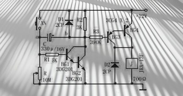
Transistor Delay Circuit
The result of mutual compensation of the potential at points A and B makes the rise of the potential at point A very small and the charging current close to seemingly constant. This carefully controlled charging process is a hallmark of a well-designed delay timer circuit, ensuring that the delay is both predictable and consistent.
When the potential at point B reaches approximately 10V, BG3 and BG4 close to cut-off, relay J is released, and the delay process ends. Press the button AN, capacitor C is quickly discharged by D1, relay J suction, and the next delay process begins , resetting the delay timer circuit for another cycle.
The delay circuit is frequently utilized, and the RC circuit is a relatively straightforward circuit. Naturally, different delay times can be achieved by adjusting the parameters of each component in the circuit. which is a key feature of the delay timer circuit, allowing for a wide range of applications and customization to specific timing requirements.


