Renesas Serves Up 100 V MOSFETs Using Split Gate Technology
Renesas has introduced new 100 V, high-power MOSFETs—the RBA300N10EANS-3UA02 and RBA300N10EHPF-5UA02— based on a new semiconductor process to help designers reach new efficiency feats.

New Renesas transistors target EVs, e-bikes, and many more applications thanks to improved efficiency and size reductions.
As global electrification continues, designers may often struggle with the physical limitations of switching efficiency, such as on-resistance or gate charge. Renesas claims its latest MOSFEET series gives designers new tools to build better and smaller power devices.
The REXFET-1 Process
At the heart of the new Renesas offerings is a new process technology, the REXFET-1, to ensure maximum efficiency.
When designing these devices, Renesas honed in on on-resistance and switching efficiency. The result is a split-gate trench architecture that reportedly improves the efficiency of resulting FETs but allows them to be integrated in a much smaller package.

Renesas' split-gate architecture is said to provide better efficiency and switching times.
The new Renesas FETs come in both TOLL (3UA02) and TOLG (5UA02) packages. Compared to standard packages such as the TO-263, the TOLL and TOLG packages are 50% smaller, allowing designers to integrate more transistors within the same real estate. The TOLL and TOLG packages are also pin-compatible with devices from other manufacturers, making it easier for engineers to make the switch.
Switching and Power Efficiency
Thanks to the split gate topology, the Ron index of the REXFET-1 transistors is pushed down to 0.24, giving designers a minimum on-resistance of 1.5 mΩ. This low on-resistance helps to reduce steady-state power loss across its wide operating range of 100 V and 340 A.
In addition to on-resistance, the REXFET-1 MOSFETs also feature improved switching performance. Qg has been reduced by 10% compared to previous generations, while Qgd has been reduced by 40%. These reductions correlate directly to faster switching, meaning more efficiency gains.
Development Resources for High-Power Designs
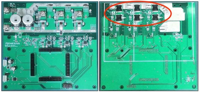
An evaluation board and two reference designs are already available for designers using the REXFET-1 process. These resources may not only help to highlight the abilities of the new Renesas transistors but also get products to market faster.

With its power transistor evaluation board, designers can get firsthand experience with the latest Renesas offerings (circled on the board).
While the difference between 2 mΩ and 1.5 mΩ may seem unassuming initially, the improvements in size and power efficiency from these new transistors are a big step toward more efficient power electronics. Renesas believes its newest transistors could find use in EVs, charging stations, data centers, and many more devices that require highly efficient transistors in a smaller form factor.


