Comprehensive Guide to MIM, MOM, and MOS Capacitors: Key Differences, Advantages, and Applications
This article provides an overview of the differences between MOM, MIM, and MOS capacitors. It covers the key characteristics, advantages, and disadvantages of each type, as well as the distinctions between them.
On-Chip Capacitors (MiM, MoM, PiP, Mos Varactor)
Catalog
I. MIM capacitor
II. MOM capacitor
III. MOS capacitor
IV. Comparison of MIM, MOM, and MOS capacitors
In analog IC circuit design, we often utilize capacitors. The capacitors inside the chip generally use metal as the upper and lower substrates. However, the disadvantage of this metal capacitor is that it consumes too much area. In some circuits that do not require very high capacitance, some people have considered using nmos transistors as an alternative.
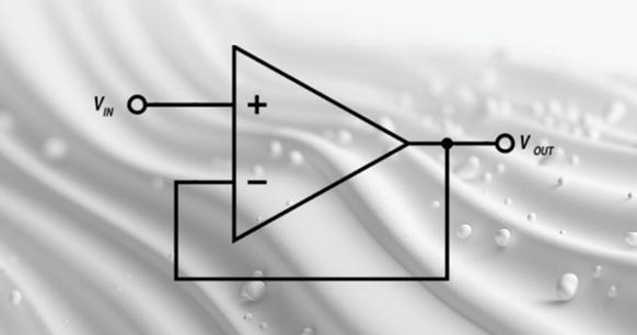
There are generally three types of integrated capacitors in CMOS technology: MIM capacitors, MOM capacitors, and MOS capacitors. Both ends of MIM and MOM capacitors are metal, with high linearity, which can be used for OPA compensation capacitors, etc. MOS capacitors, which can also be referred to as mosfet capacitors, generally require grounding or power at one end. The linearity of MOS capacitors is not as high as that of other types. They are typically used for larger capacitors that require filtering.
I. MIM capacitor
MIM capacitor (Metal-Insulator-Metal): MIM capacitors are equivalent to parallel plate capacitors. The two-layer metal on the top layer has a large spacing, and the formed capacitor has a small capacitance value.
The structure of the MIM capacitor is as follows: the dielectric layer between CTM and Mt-1 is relatively thin, resulting in a higher-density capacitor.
MIM capacitors are formed using different layers of metals and a dielectric material.
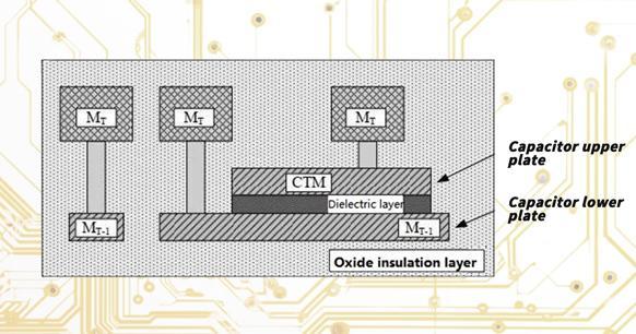
MIM capacitor structure
Advantages of MIM capacitors: MIM capacitor structure Special processes can be used to connect odd-numbered layers (M9, M7, M5) and even-numbered layers (M8, M6, M4), respectively, which can increase the unit area capacitors.
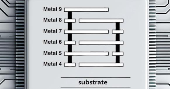
MIM structure metal4-metal9
Disadvantages of MIM capacitors: In the 65nm process, even if the upper 9 layers of metal and poly are used to build MIM, the unit area capacitor is only (1.4fF/micron square). It should be noted that the parasitic capacitor Cp can reach 10% of the total capacitor.
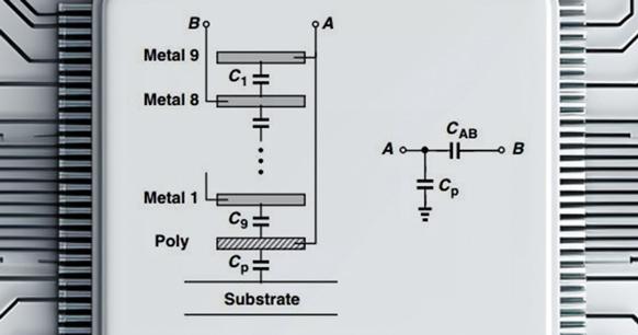
MIM circuit
II. MOM Capacitor (Metal-Oxide-Metal):
MOM capacitors, a type of MOM cap, are generally interdigitated capacitors formed by MOM metal connections. The structure is designed to take advantage of the Metal-Oxide-Metal configuration, which allows for a high-density arrangement of the capacitors. With the advancement of process technology, the MOM metal wires can be placed closer together, and the availability of multiple metal layers increases the capacitor density of this structure under advanced technology.
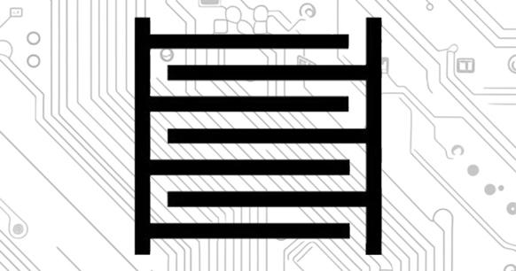
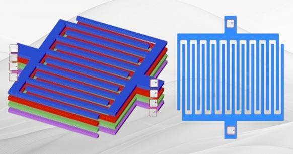
MOM structure
Different from MIM capacitors, MOM capacitors mainly use the same-layer MOM metal interdigital structure to construct capacitors, offering several distinct advantages:
- High unit capacitance: The interdigitated structure of MOM capacitors allows for a higher capacitance per unit area.
- Low parasitic capacitor: The design of MOM capacitors minimizes the impact of parasitic capacitance, leading to better performance.
- Symmetrical plane structure: The symmetry of MOM capacitors contributes to improved stability and reliability.
- Excellent RF characteristics: The structure of MOM capacitors is well-suited for radio frequency applications due to its low loss and high-frequency response.
- Excellent matching characteristics: The consistency in the manufacturing process ensures capacitors with matching properties, which is crucial for precision circuits.
- Compatible with metal wire process: MOM capacitors can be integrated without the need for additional processes, streamlining manufacturing.
In the advanced CMOS manufacturing process, MOM capacitors have become the most important capacitor structure. In the 28nm process, fixed capacitors have taken on the MOM form exclusively, highlighting the significance and prevalence of MOM caps in contemporary semiconductor technology.
III. MOS Capacitor
The MOS capacitor (metal-oxide-semiconductor) is the central component of the MOSFET structure. While not a widely used device in itself, the MOS capacitor forms the core unit of the entire MOSFET, which includes both nmos and pmos transistors.
The gate capacitor of the MOSFET, which is also known as the nmos transistor, can achieve a higher capacitor density. However, the capacitance value will vary with the difference of the gate voltage, which has a relatively large non-linearity.
Understanding mosfet equations is crucial for analyzing the behavior of these capacitors, which can be compared with traditional bipolar junction transistors (BJTs) in a mosfet vs transistor discussion. The gate, drain, and source are the three main terminals of a MOSFET, and their interactions are governed by the mosfet gate drain source relationships.
In the inversion zone, a significant number of inversion minority carriers are formed within the gate oxide layer. Similarly, a considerable number of multi-carriers are generated in the accumulation region. In both of these operational zones, the MOS structure exhibits characteristics similar to those of a parallel plate capacitor. This results in a capacitance value that is approximately equal to the gate oxide capacitor Cox.
As illustrated in the accompanying figure, this is a graph of the capacitance value of the MOSFET with the gate voltage. In order to achieve optimal linearity, the MOS capacitor must operate in the inversion region, that is, Vgs > Vth.
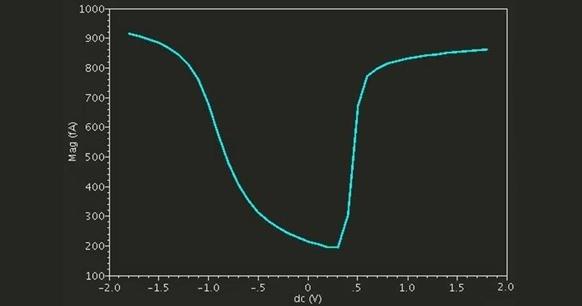
Variation of MOS capacitance with gate voltage
Physical Structure
MOS capacitors are comprised of three layers: an upper gate made of metal, a lower substrate made of semiconductor, and a middle layer filled with oxide, typically SiO2. It has only two ports: gate and substrate. The schematic diagram is provided below:
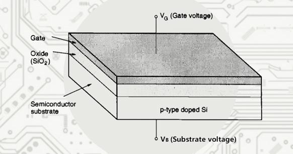
MOS Capacitor Structure
The structure of a P-type semiconductor MOS capacitor is as follows: The topmost metal layer, referred to as the gate, applies a negative bias voltage to the P-type semiconductor situated on the substrate. The metal end of the gate accumulates negative charges, creating an electric field.
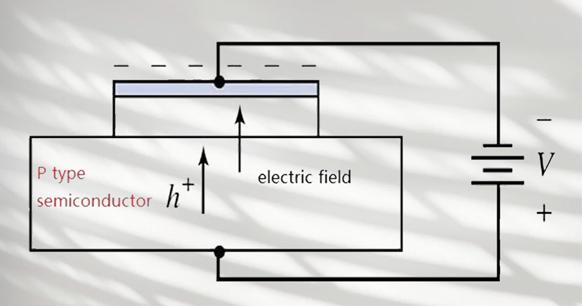
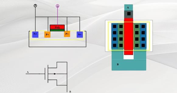
PMOS capacitor
The mechanism of the N-type semiconductor MOS capacitor is similar to that of the P-type semiconductor MOS capacitor. The figure below shows a schematic diagram of the structure of an N-type semiconductor MOS capacitor. When a forward bias voltage is applied at the gate level, a positive charge is generated at the gate level, a corresponding electric field is induced, and an electron accumulation layer is formed at the oxide-semiconductor interface.
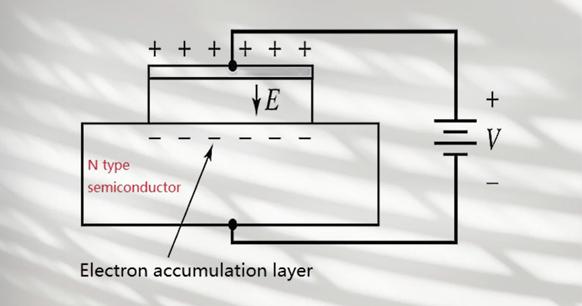
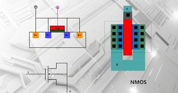
NMOS capacitor
In some processes, to avoid inversion, special MOSFETs form MOS capacitors, with NMOS transistors placed in the n-well. When the gate voltage is 0, the MOS tube is already turned on, and the threshold voltage Vth is close to 0. When Vgs > 0, the capacitance value tends to be stable. This structure is called an accumulation type MOS capacitor, often referred to as a native MOS. The figure below shows the structure of this type of capacitor.
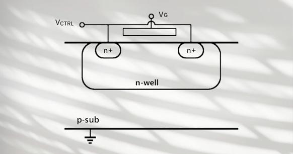
Accumulation type MOS capacitor structure
The accumulation type MOS capacitor structure is based on the principle of a MOSFET. The main principle of a MOSFET is to form a capacitor by using the gate oxide between the gate and the channel as the insulating medium. The gate is used as the upper plate, and the three ends of the source and drain and the substrate are shorted together to form the lower plate.
When the power of the gate is sufficient to exceed the threshold voltage Vth, an inversion layer will form between the source and the drain, facilitating channel formation. The MOS capacitor's unit area size is related to the thickness and dielectric constant of the gate oxide.
If the gate voltage is unable to form a channel between the source and drain or cause holes in the P-type substrate to accumulate on the top, a space charge region will form under the gate oxide. This space charge region, formed by the combination of electrons and holes, acts as an insulator, affecting the capacitance value.
The advantages and disadvantages of MOS capacitors are as follows: They offer area-saving and convenience but are less suitable for high-precision circuits due to their "voltage-controlled" nature, which can be a significant issue in weak signal acquisition applications.
IV. Comparison of MIM, MOM, and MOS capacitors
MIM capacitors: similar to plate capacitors, the capacitance value is more accurate, and the capacitance value does not change with the bias voltage. In general, mTOP l and mTOP -1 are used in the manufacturing process. The capacitance value can be estimated by multiplying the upper board area by the unit capacitance value. It should be noted that the upper and lower plate connections are not interchangeable and are generally used in analog and RF processes.
MOM capacitors are interdigital capacitors that use C between the edges of the same layer of metal. To optimize space, multiple layers of metal can be stacked, and the number of metal layers in PDK can be selected. MOM capacitors are typically utilized in advanced manufacturing processes of multilayer metals. As it is realized through the layout of multilayer wiring, the determinism and stability of the capacitance value obtained are not as good as MIM. It is generally used in applications that do not require high capacitance values.
The MOS transistor with two ends structure has an inaccurate capacitance value. It can achieve a capacitance value that changes with the change of the control voltage, and the connection of the upper and lower plates is not interchangeable.
A comparison of the capacitance values of three capacitors with the same area shows that MIM is approximately one-third of the MOS capacitance value.
One advantage of the MOM capacitor is that no additional mask is required, whereas MIM requires an additional mask and process to be realized.


