


Overview
The 74LVC594APW-Q100118 is an 8-bit serial-in/serial or parallel-out shift register with a storage register, manufactured by NXP USA Inc. (now part of Nexperia). This device is designed for use in a variety of digital logic applications, offering flexibility in data transfer and storage. It features separate clock and reset inputs for both the shift and storage registers, enabling precise control over data movement.
Key Specifications
| Parameter | Value |
|---|---|
| Type Number | 74LVC594APW |
| VCC (V) | 1.2 - 3.6 |
| Logic Switching Levels | CMOS/LVTTL |
| Output Drive Capability (mA) | ± 24 |
| tpd (ns) | 3.1 |
| fmax (MHz) | 180 |
| Number of Bits | 8 |
| Power Dissipation Considerations | Low power dissipation |
| Tamb (°C) | -40 to +125 |
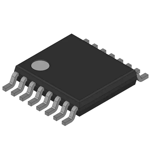
| Package Name | TSSOP16 (SOT403-1) |
Key Features
- Serial-In/Serial or Parallel-Out Shift Register: Allows for flexible data transfer modes.
- Separate Clock and Reset Inputs: For both shift and storage registers, providing precise control.
- Schmitt-Trigger Action at All Inputs: Enhances tolerance to slower input rise and fall times.
- Wide Supply Voltage Range: From 1.2 V to 3.6 V, making it suitable for various power environments.
- Overvoltage Tolerant Inputs: Up to 5.5 V, ensuring robustness against voltage spikes.
- CMOS Low Power Dissipation: Minimizes power consumption.
- Direct Interface with TTL Levels: Compatible with TTL logic levels.
- IOFF Circuitry: Enables partial power-down mode operation, preventing backflow current when powered down.
- ESD Protection: HBM (ANSI/ESDA/JEDEC JS-001 class 2) exceeds 2000 V and CDM (ANSI/ESDA/JEDEC JS-002 class C3) exceeds 1000 V.
Applications
The 74LVC594APW-Q100118 is suitable for a variety of applications, including:
- Digital Logic Circuits: Where serial-to-parallel data conversion is required.
- Mixed Voltage Environments: Acts as a translator between 3.3 V and 5 V devices.
- Remote Control Systems: Can be used in holding registers for remote control applications.
- Automotive and Industrial Systems: Due to its robust ESD protection and wide operating temperature range.
Q & A
- What is the primary function of the 74LVC594APW-Q100118?
The primary function is to act as an 8-bit serial-in/serial or parallel-out shift register with a storage register.
- What is the voltage range for the VCC of this device?
The voltage range for VCC is from 1.2 V to 3.6 V.
- What type of logic switching levels does this device support?
The device supports CMOS and LVTTL logic switching levels.
- What is the maximum output drive capability of this device?
The maximum output drive capability is ± 24 mA.
- What is the maximum propagation delay (tpd) of this device?
The maximum propagation delay is 3.1 ns.
- What is the maximum clock frequency (fmax) supported by this device?
The maximum clock frequency is 180 MHz.
- What type of package is the 74LVC594APW-Q100118 available in?
The device is available in a TSSOP16 (SOT403-1) package.
- Does the 74LVC594APW-Q100118 have ESD protection?
Yes, it has ESD protection with HBM exceeding 2000 V and CDM exceeding 1000 V.
- What is the operating temperature range for this device?
The operating temperature range is from -40 °C to +125 °C.
- Can the 74LVC594APW-Q100118 be used in mixed voltage environments?
Yes, it can be used as a translator between 3.3 V and 5 V devices.


