Revolutionizing Wireless Amplification: The Complete Guide to RF Power LDMOS Transistors

Catalog
1.Advancing Wireless Communication: The Role and Evolution of RF Power Amplifiers
2.LDMOS Transistors: The Backbone of Modern Wireless Communication
3.Evolution of RF Power Amplifiers: From Vacuum Tubes to LDMOS Technology"
4.LDMOS vs. GaN: The Strategic Choice for RF Power Amplifiers in Modern Wireless Communications
5.RF Power LDMOS Transistors: The Optimized Choice for High-Frequency Wireless Amplification
6.MRFE6VP100HR5: A Superior Solution for RF Power Amplifiers
1.Advancing Wireless Communication: The Role and Evolution of RF Power Amplifiers
In the realm of wireless communication, the power amplifier is a crucial component of the entire system. It is responsible for amplifying the input signal to the required power level, providing sufficient drive capability for the antenna. Compared to traditional power amplifiers, RF power amplifiers exhibit several advantageous characteristics within higher frequency bands, including higher output power, higher efficiency, and higher reliability. They act as a core component in RF front-end architectures for a variety of applications, such as base stations, mobile phones, WiFi, NB-IoT, and other domains of wireless communication. Moreover, they can be integrated into RF power sources for use in industrial, medical, scientific, and other sectors.

Applications of RF Power Amplifiers
As communication technology continuously evolves, the performance requirements for power amplifiers are becoming increasingly demanding. There is a need for higher power output, wider bandwidth, greater efficiency, and stronger anti-interference capabilities. To meet these stringent demands, semiconductor manufacturers are constantly introducing new types of power amplifier devices. Among these, RF Power LDMOS Transistors stand out as an exceptional representation.
2.LDMOS Transistors: The Backbone of Modern Wireless Communication
Introduction
LDMOS, or Laterally Diffused Metal Oxide Semiconductor, is a specialized power semiconductor device structure renowned for its role in RF power amplifiers within the wireless communication sector. The unique layout of LDMOS transistors positions the drain and source on the silicon wafer's plane, while the gate stands perpendicular to the wafer's surface. This architectural advantage endows LDMOS transistors with lower on-resistance and higher breakdown voltage, making them ideal for designing power amplifiers.
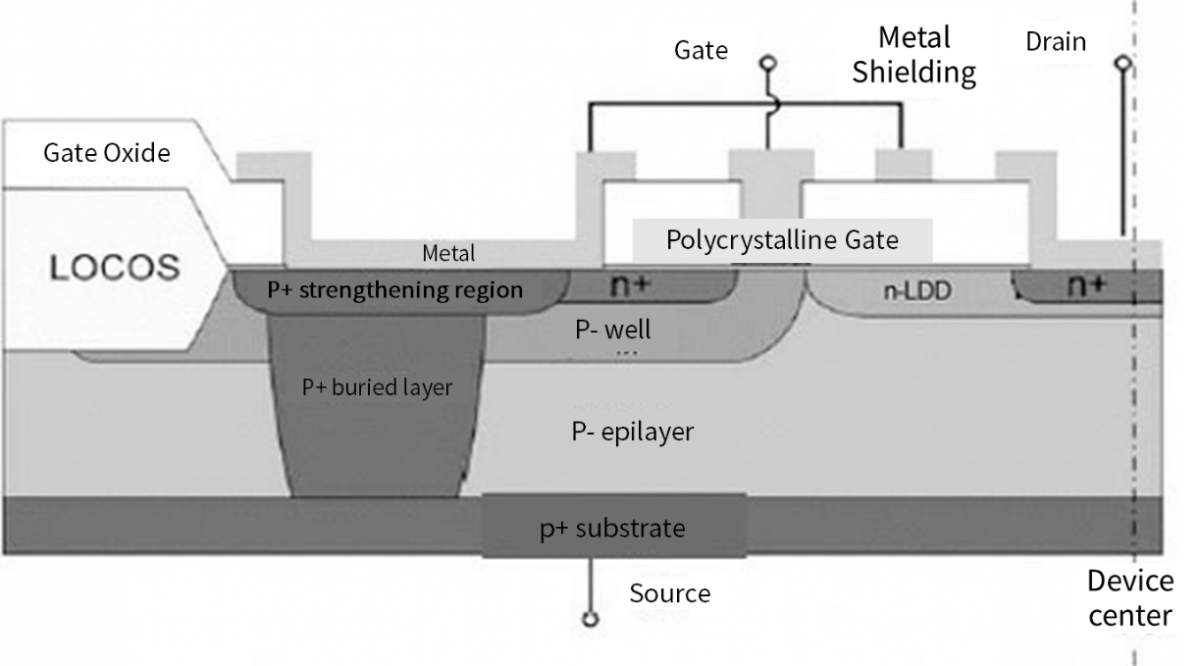
Principle Structure Diagram of RF Power LDMOS Transistors
Advantages of LDMOS in Wireless Communication
LDMOS technology has become one of the most widely adopted power semiconductor technologies in the wireless communication field. When compared to traditional Si MOSFETs and GaAs FETs, LDMOS transistors offer superior characteristics such as higher breakdown voltage, lower conduction resistance, and enhanced thermal management capabilities. These attributes make LDMOS particularly suitable for high-power and high-frequency wireless communication systems, including 5G base stations, radar systems, and satellite communications.
Applications in Telecommunications
In the domain of telecommunications, LDMOS RF power amplifiers are extensively utilized in base stations and mobile radios. They are favored for their cost-effectiveness, high integration levels, and improved compatibility with Digital Pre-Distortion (DPD) technology. Among various applications, communication base stations represent the largest area of implementation for LDMOS technology.
3.Evolution of RF Power Amplifiers: From Vacuum Tubes to LDMOS Technology
In the early days of wireless communication systems, power amplification was predominantly achieved using vacuum tube technology. While capable of delivering high power outputs, vacuum tubes were constrained by their large size, low efficiency, and short lifespan, which limited their application in modern communication systems.
In the 1960s, with the advancement of semiconductor technology, RF power transistors gradually supplanted vacuum tubes as the primary device for power amplification. The initial RF power transistors were based on the bipolar structure, known as BJTs (Bipolar Junction Transistors). BJTs offered high power gain and power density but were hindered by their slow switching speeds, which restricted their performance at high frequencies.
To enhance the bandwidth and efficiency of RF power amplifiers, MOSFETs (Metal-Oxide-Semiconductor Field-Effect Transistors), which are based on a field-effect structure, were developed. MOSFETs are characterized by their fast switching speeds and low power consumption, making them highly suitable for high-frequency applications. Among them, LDMOS (lateral diffused metal-oxide-semiconductor) is a specialized type of MOSFET structure. It features a layout where the source and drain are positioned on either side of the transistor, enabling it to withstand higher drain-source voltages and making it exceptionally suitable for power amplification.
4.LDMOS vs. GaN: The Strategic Choice for RF Power Amplifiers in Modern Wireless Communications
As communication frequency bands continue to rise, the manufacturing of RF power transistors has embraced advanced materials like Gallium Nitride (GaN) and Silicon Carbide (SiC). These wide-bandgap semiconductors offer higher breakdown voltages, increased power density, and improved thermal management capabilities, paving the way for RF power amplifiers that can operate at higher frequencies and power levels.
In the current landscape, LDMOS, GaN, and SiC technologies coexist, each with its own set of advantages and disadvantages, and are utilized across various wireless communication systems. LDMOS, known for its mature manufacturing process, cost-effectiveness, and favorable linearity, is predominantly used for power amplification in the mid to low-frequency bands, as seen in 2G/3G/4G base stations and broadcast transmitters. On the other hand, GaN and SiC, with their superior high-frequency performance and power density, are more suited for high-frequency applications such as radar and satellite communications.
Since the advent of 2G mobile communication technology, LDMOS has become the dominant choice in base station applications and continues to hold this position. With the evolution of 4G and 5G technologies, GaN has gained widespread adoption in base stations for its exceptional performance in high-frequency applications. Despite this, LDMOS maintains its relevance in medium and low-frequency applications, benefiting from its low cost, high integration, and better compatibility with Digital Pre-Distortion (DPD) technology. In scenarios where power is limited, such as in pre-driver stages and small base stations, Gallium Arsenide (GaAs) remains in use, although its market share is diminishing.
The selection between GaN and LDMOS is influenced by their distinct advantages and is often a dynamic decision based on the Original Equipment Manufacturer's (OEM) strategy. GaN is typically favored for high-frequency, high-power applications, whereas LDMOS is utilized in medium and low-frequency scenarios. LDMOS also finds a niche in certain high-frequency, low-power applications. As wireless communication technology advances, both GaN and LDMOS continue to play crucial roles in shaping the future of RF power amplifiers for base stations and beyond.
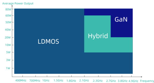
Different Application Ranges of LDMOS and GaN Based onFrequency and Power
5.RF Power LDMOS Transistors: The Optimized Choice for High-Frequency Wireless Amplification
What are RF Power LDMOS Transistors?
RF Power LDMOS Transistors are devices optimized for power amplification applications in the field of wireless communication, building upon the foundation of LDMOS technology. They possess several key features:
1) Broad Frequency Range: Operating from 1.8 MHz to 2000 MHz, RF Power LDMOS Transistors meet the demands of various applications, from ISM (Industrial, Scientific, and Medical) bands to broadcast television frequencies.
2) High Power Output: Capable of delivering up to 100 watts of CW (Continuous Wave) output power from a single device, these transistors are designed to drive high-power antenna arrays.
3) High Efficiency: With over 70% drain efficiency at 100 watts CW output power, these devices significantly reduce power consumption and heat dissipation requirements.
4) High Reliability: Employing Freescale's enhanced voltage tolerance technology, RF Power LDMOS Transistors can withstand load mismatches as high as 65:1, maintaining stable and reliable performance even under adverse operating conditions.
5) Integrated Design: These devices integrate stability enhancement circuits and ESD protection features, simplifying the design complexity of power amplifiers.
6.MRFE6VP100HR5: A Superior Solution for RF Power Amplifiers
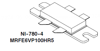
The MRFE6VP100HR5 is an RF Power LDMOS Transistor specifically designed by Freescale for wireless communication applications within the 1.8 MHz to 2000 MHz frequency range. It offers several significant advantages:
1) Broad Frequency Characteristics: With its ultra-wide frequency range covering ISM bands to broadcast television bands, the MRFE6VP100HR5 allows designers to implement power amplifiers for multiple frequency bands using the same device, simplifying the design process and reducing costs.
2) High Power Output: This transistor can provide up to 100 watts of CW output power per device, sufficient to drive large antenna arrays. In pulsed operation, the peak output power can even reach 130 watts, making it ideal for high-power wireless communication systems.
3) High Efficiency: Achieving over 70% drain efficiency at 100 watts CW output power, the MRFE6VP100HR5's industry-leading efficiency significantly reduces power consumption and heat dissipation, enhancing the energy efficiency of the entire system.
4) High Reliability: Featuring Freescale's robust voltage tolerance technology, the MRFE6VP100HR5 can endure load mismatches of up to 65:1, ensuring stable and reliable operation even under severe antenna mismatch conditions, which extends the system's service life and reliability.
5) Integrated Design: The internal integration of stability enhancement circuits and ESD protection circuits in the MRFE6VP100HR5 reduces the complexity of peripheral circuit design. Additionally, the device provides comprehensive parameter testing data, including thermal resistance and ESD characteristics, offering design engineers a wealth of reference information and further simplifying the design of power amplifiers.
References:
ICV: 2023 LDMOS RF Power Amplifier for Base Stations China Market Research Report