Rethinking MCU Architectures for the AI Era
There will always be a market for traditional microcontrollers (MCUs) that perform embedded control functions without any native artificial intelligence (AI) capability. But the rapidly growing need to perform AI functions at the endpoint is increasingly going to dictate the specification of MCUs for use in new product designs. This is illustrated at the macro level in Figure 1.
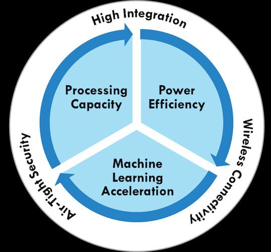
Figure 1. Essential components for a successful AI-capable MCU
The battle in the MCU market is increasingly going to be won by those who can integrate neural processing unit (NPU) capability closely coupled to conventional MCU features and functions. The architecture that the MCU manufacturer adopts for this new type of hybrid CPU/NPU device has real implications for OEMs’ product designs, affecting their performance and response times, their power consumption, and the productivity of the engineering teams that develop the products.
Demands From End Customers
All of this leads to the satisfaction of the end consumers who expect to experience fluid and useful functionality without perceivable delay at an affordable price in products such as wearables, hearables, fitness and health monitors, smart cameras, and gaming with less dependency on the cloud.
Engineers who are tasked with selecting an AI-capable MCU will of course rely on performance benchmarks and other technical data—but they will also benefit from looking underneath the hood at the way the NPU has been integrated into the familiar embedded controller’s structure.
MCU Battle Moves On To New Ground
Arguments over rival implementations of neural networking capability in MCUs have not yet burst into the open, simply because so few manufacturers have meaningfully addressed the market need for effective machine learning (ML) capability in endpoint IoT devices.
The giants of the MCU market have by and large preferred to enhance existing portfolios by adding ML features to their software development kits (SDK), while maintaining largely unchanged legacy silicon IP. This IP in nearly all cases is anchored in older generations of the Cortex-M CPU architecture from Arm to execute the ML workload, while in rare cases a proprietary neural networking co-processor is employed.
On top of that, traditional internal memory implementations are being used that are undersized, over-shared, and not placed in proper proximity to neural processing activity to resolve ML inferences at the desired rate and power consumption. When forced to use off-chip memory, the system cost, size and power consumption go up while the level of security goes down.
Optimized NPU Hardware is Vital
This position is not going to hold. Practical experience is showing MCU users that neural networking operations map poorly on to control-oriented RISC CPUs at the heart of a traditional MCUs. To stay within the power budget and to meet performance requirements, an MCU for endpoint applications needs NPU hardware optimized for multiply accumulate (MAC) operations that are the bread and butter of neural networking applications, and connected to memory with extremely high bandwidth.
The table in Figure 2 highlights the case in point. Let’s examine Alif Semiconductor’s Ensemble MCU family. The MCUs employ the contemporary Cortex-M55 CPU core, which includes the Single Instruction-Multiple Data (SIMD) vector processing extension called Helium, paired with an Ethos-U55 NPU co-processor. In fact, many Ensemble MCUs use two pairs of Cortex-M55 CPU+Ethos-U55 NPU, but more on that later.

Figure 2. Benchmark tests show the superior performance and efficiency uplift when using an NPU to accelerate common ML workloads. See Figure 2 footnotes at the end of the article. (Click image to enlarge)
The table shows you metrics for a single ML inference for four different trained ML models running on an Ensemble MCU representing keyword spotting, object detection, image classification, and speech recognition. Moving left to right, the green area indicates when the ML model workload is being executed using all the available hardware acceleration—the Ethos-U55 NPU plus the Cortex-M55 CPU while using its SIMD vector instruction set.
The yellow area shows these metrics again after removing help from the Ethos-U55 NPU. The blue area shows the metrics while CPU-bound, meaning no hardware assistance, just the CPU alone.
Finally, relative performance improvements are shown at the right side with the green area highlighting the performance uplift contributed by using all available acceleration compared to the CPU with SIMD; the yellow highlighting uplift contributed by the CPU with SIMD vs just the CPU without SIMD; and finally the blue showing uplift contributed by full acceleration vs no acceleration.
A Look At The Comparisons
Referring again to the table in Figure 2 above, Here's what can be learned from these comparisons:
- Blue Areas—An embedded CPU on its own will struggle with meaningful ML workloads because inferences derived from the highly parallel ML network must be resolved in a serial fashion, taking excessive time while consuming a lot of energy. The Cortex-M55 is among the best embedded CPU architectures and puts up good numbers that are already on the order of 5x better for ML workloads than previous generations of Cortex-M CPU cores. However, even as good as the Cortex-M55 is, look at the excellent additional performance uplift shown in the far right blue area, exceeding or approaching a two orders of magnitude uplift when using full acceleration vs the CPU only. And if you consider that Cortex-M55 already performs around five times better than other widely used Cortex-M architectures, you can generally multiply these gains again by 5x. For speech recognition that is around 800x faster and 400x less energy per inference.
- Yellow Areas—Bringing SIMD-based vectorized math capabilities to the MCU space affords substantial performance and power improvements compared to just the CPU alone, because it allows for more parallel processing. The Helium M-Profile Vector Extension (MVE) was ushered into this space with the Cortex-M55 CPU Armv8.1-M architecture.
- Green Areas—Here is where a dedicated NPU co-processor shines. The ML workload is split by the compiler between the NPU and the CPU, with typically 95% or more of the ML workload landing on the NPU, depending on the ML model. The NPU generates inferences extremely fast and efficiently by performing MAC operations in hardware in a massively parallel fashion. As an important side benefit, while the NPU is working, the CPU can go to sleep to save energy or perform other tasks.
Over time, all MCUs for use in endpoint ML applications are going to become hybrid CPU/NPU devices. It’s as inevitable as other basic trends in the MCU world over the past decades, such as the move to Flash memory-based MCUs, and the integration of USB connectivity in almost every MCU.
Evaluating MCU Architectures: New Options
So then the question is going to be, how do MCU manufacturers’ architectural choices about integrating the neural networking capability affect OEMs’ development teams?
Alif has some early insight into the answer. The company was the first MCU manufacturer to bring to market a scalable family of controllers and wireless MCUs that combine a Cortex-M CPU with an Arm Ethos-U NPU.
Here are the three most important aspects of the hybrid CPU/NPU architecture that, in our experience, OEM developers should study when they choose an MCU for endpoint ML applications.
- Fast, low-power ML inferencing depends on memory type and topology.
- Maximizing battery life
- Enhancing developer productivity
Let’s examine each of these points in detail one-by-one.
1- Memory Type and Topology
OEMs will in many cases be implementing ML at the endpoint because the application demands a response that the user perceives as instant. Also, the majority of these products will be portable and wireless, so long life from small batteries is critical.
We saw from Figure 2 that enhanced processing capability is key to high performance and power efficiency, but without an optimized memory system behind it the results will fail to meet expectations.
A simplified view of the Ensemble MCU memory topology is shown in Figure 3. The upper half represents the real-time section, with very fast Tightly Coupled Memory (TCM) connected to the CPU and NPU cores. For fast (low latency) inferences, these TCM SRAM memories must be sufficiently large to hold the ML model’s tensor arena.
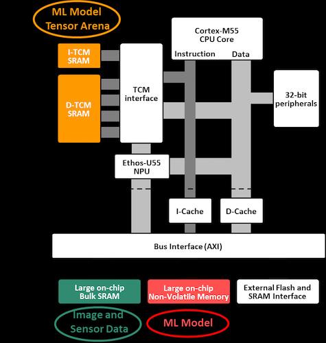
Figure 3. The Ensemble MCUs’ internal memory topology
The lower half of the diagram shows other memories distributed about the system, and connected by a common high-speed bus. A large bulk SRAM is required to hold sensor data, such as the input from a camera and microphones, and a large non-volatile memory contains the ML model itself plus application code. When large on-chip memories are distributed this way to minimize competing bus traffic, then concurrent memory transactions flourish, bottlenecks are cleared, memory access times are minimized, and power consumption is compatible with the use of a small battery.
Keep in mind that within embedded ML systems, a large portion of the energy consumed to generate an inference comes from moving data from place to place. In systems that have under-sized memories with poor memory topology, the energy consumed just to move the data back and forth can exceed that consumed by CPU and NPU processing functions.
Further, if spillover data or code requirements force the use of an external off-chip memory, then energy requirements can increase by an order of magnitude, and also expose sensitive code and ML model IP to a potential security breach.
2- Maximizing Battery Life
Alif recognized early on that the concentration of local ML capability at the endpoint will skyrocket in the very near future while at the same time the physical size of these products will rapidly shrink, especially for wearables. Smart glasses, fitness rings, and hearing enhancers are examples of AI-enabled wearable devices for which market demand is expected to grow dramatically. All need to be powered by a smaller battery.
Alif’s approach to stretching battery life took several forms. Two examples are:
- Partitioning the system so that a low-power portion of the chip can be always-on. This always-on segment offers robust compute capability, enabling it to selectively wake a much higher performance portion of the chip to execute heavy workloads then return to sleep
- The power management system dynamically powers on only portions of the chip that are needed and shuts them off when not.
Many Ensemble MCUs have two pairs of Cortex-M55+Ethos-U55 cores as shown in Figure 4:
- One in the High-Efficiency region of the chip built on low-leakage transistors that can be always-on operating at up to 160 MHz
- The other pair in the High-Performance region operating at up to 400 MHz.
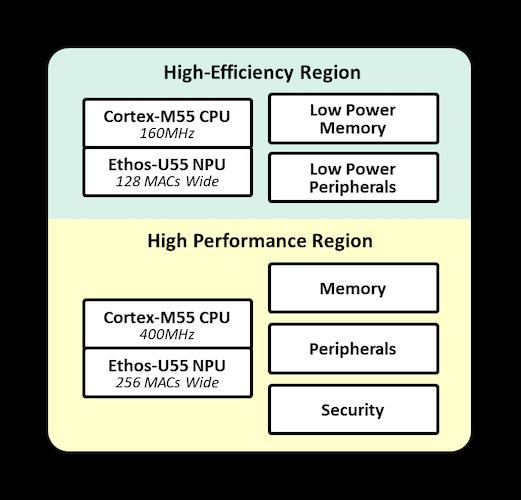
Figure 4. Ensemble E3 MCU block diagram showing the High-Efficiency and High-Performance regions of the chip
To picture the advantage this brings, think of a smart occupancy camera that continuously scans a room at a low frame rate using the High-Efficiency pair to classify a valid event (such as a human falling to the floor, or a specific gesture) which wakes the High-Performance pair to identify a person or persons, check for blocked exits, dial for help, and so on.
In this case the camera can be intelligently vigilant, produce less false positives, and extend battery life. Similar uses for these two pairs of CPU+NPU cores can be applied just as relevantly to the classification of sounds, voices, words, OCR text, vibrations, and sensor data in many varied applications.
All Ensemble MCUs also employ Alif’s aiPM (autonomous intelligent Power Management) technology to manipulate in real time up to 12 individual power domains in the chip as needed to match the use case being executed.
Only domains that are actively executing tasks are powered on (such as those powering specific processing cores, memories, or peripherals) while the other domains remain off. This becomes transparent to the software developer.
3- Enhancing Developer Productivity
For many engineers who are steeped in the ways of real-time embedded control, AI systems are an unfamiliar domain which requires a new approach to software development. But the unfamiliarity does not need to extend to the development environment itself.
The MCU world has standardized on the Arm Cortex-M architecture for embedded control, and now Arm’s Ethos NPUs are joining that robust support ecosystem and enjoying all its familiar benefits. But in the field of embedded NPU engines, a wide choice of other products is available from IP vendors, and some well-known MCU manufacturers are creating their own proprietary NPU IP.
AI Development in an MCU Environment
All these other choices, however, take the NPU outside the Arm ecosystem in which embedded control functions are developed. This makes the Ethos NPU a better choice for many users, since it allows AI functions to be developed in the same familiar MCU environment as used for control functions.
In an Ensemble MCU, for example, the Ethos NPU essentially functions as a smart peripheral of a Cortex-M55 CPU to which it is closely tied, sharing TCM resources which are marshaled by the Cortex core. This means that the developer does not need to worry about hardware resource allocation. The Arm compiler simply portions out the ML workload appropriately to the NPU and CPU without requiring specific allocation instructions from the developer.
A further advantage of using an Ethos NPU is that Arm undertakes to maintain it, so that it is always up to date, and supports the latest instance of whichever framework – such as TensorFlow Lite – the developer chooses to use to build their ML model. Arm’s support for the Ethos NPU ensures that developers are not restricted in their choice of ML framework.
New Architectures For New Requirements
Although there are many, this article describes three of the most important grounds on which the battle to provide MCUs for ML at the endpoint look set to be fought. Alif arrived early on the scene to provide MCUs that include strong endpoint ML capabilities, while also keeping in mind robust security, the correct mix of peripherals and interfaces, wireless connectivity, and offering a wide selection of scalable and compatible devices ranging from a single CPU core for RTOS to quad-core devices that also support the Linux operating system.
What Alif has learned in pioneering the development of hybrid Cortex-M/Ethos MCUs could help OEM developers to decide which features and characteristics their chosen MCU should include when AI/ML makes its way to the top of their application requirements.
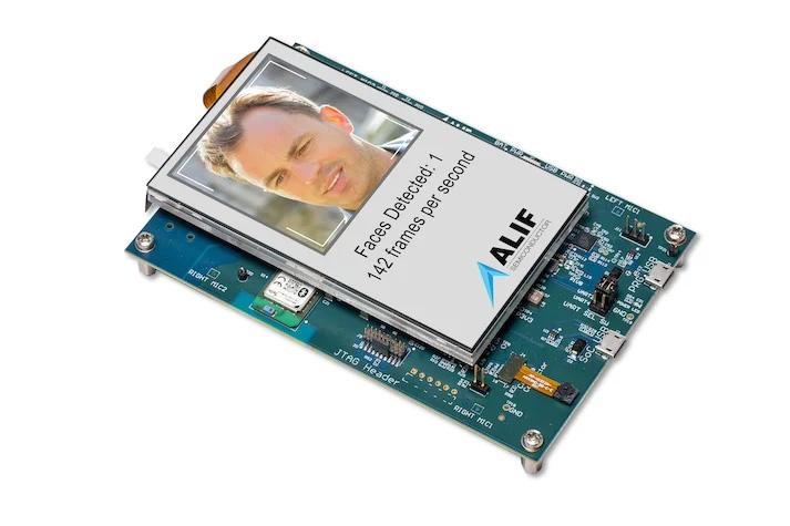
Figure 5. Alif Ensemble AI/ML AppKit, AK-E7-AIML
Alif will continue to be at the forefront in this market by introducing the first MCUs to use Arm’s next generation Ethos-U85 NPU, which will support transformer-based ML models for generative AI applications at the endpoint.
And today, developers can learn more about the Ensemble family of devices at Alif Semiconductor’s website, and start working with the devices with the Ensemble AI/ML AppKit (Figure 5). The kit includes the Ensemble E7 fusion processor, a camera, microphones, a motion sensor, and a color display.
All images used courtesy of Alif Semiconductor
Footnotes to Figure 2:
- KWS: From Arm MicroNets paper. Quantized int8, trained on ‘Google Speech Commands’ dataset. Model footprint: 154 KB MRAM, 28KB SRAM
- Object Detection: 192 x 192 grayscale resolution and color. Quantized int8, trained on ‘WIDER FACE’ dataset. Model footprint: 431 KB MRAM, 433 KB SRAM
- Image Classification: 224 x 224 24-bit resolution % color. Quantized int8, trained on ‘ImageNet’ dataset. Model footprint: 3,552KB MRAM, 1,47 KB SRAM
- ASR: Tiny Wav2letter Pruned slotted into ARM's ML demo app, running the ASR use case. MRAM =2 346.06 KB (greatly Vela optimized from 3903.43 KB), SRAM=1197.20 KB
Industry Articles are a form of content that allows industry partners to share useful news, messages, and technology with All About Circuits readers in a way editorial content is not well suited to. All Industry Articles are subject to strict editorial guidelines with the intention of offering readers useful news, technical expertise, or stories. The viewpoints and opinions expressed in Industry Articles are those of the partner and not necessarily those of All About Circuits or its writers.

