NXP Rolls Out Automotive MCU for Zonal SDVs, Leveraging MRAM
Today, at the start of Embedded World 2025, is introducing the S32K5, a new microcontroller family designed to accelerate the transition to zonal architectures in automotive design. All About Circuits had the chance to talk with David Vieira, Zonal Segment Lead for Automotive at NXP, to learn about the new MCU firsthand.

Jeff Child at NXPs Embedded World booth with David Vieira, Zonal Segment Lead for Automotive, learning about NXPs new S32K5 automotive microcontroller. Image used courtesy of Jeff Child.
The S32K5
According to NXP, the S32K5 is the industry’s first automotive MCU that is built on a 16 nm FinFET process and integrates embedded magnetic RAM (MRAM) in place of conventional embedded flash storage. Ultimately, the goal of the new MCU is to consolidate electronic control unit (ECU) functions while maintaining deterministic low-latency communication, safety measures, and efficient real-time processing.
As Vieira tells us, “These are high-performance, low-latency real-time computing control MCUs. We’re addressing zonal architectures as well as X and Y electrification use cases. This MCU family is really designed to enable a smooth transition from distributed ECUs to a zonal model.”
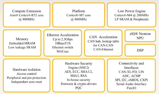
Block diagram of the S32K5 MCU. Image used courtesy of NXP Semiconductors
NXP is doing this by making the S32K5 an extension of its CoreRide platform so that automakers can scale their software-defined vehicle (SDV) architectures with pre-integrated software and reference solutions. As part of this, the MCU features Arm Cortex-R52 and Cortex-M7 cores running at up to 800 MHz, an integrated 2.5 Gbps Ethernet switch, CAN-XL support, and a post-quantum cryptography (PQC)-ready security engine.
MRAM Integration and the Elimination of Embedded Flash
One of the most significant architectural changes in the S32K5 is the use of embedded MRAM instead of traditional embedded flash. In this process, NXP bypassed the 28nm node and transitioned directly from 40 nm to 16 nm FinFET, where embedded flash is no longer a viable option. This shift required selecting a non-volatile memory technology capable of delivering high-speed writes, durability, and long-term reliability.
Vieira explains puts this trend into perspective.
“When you get to 16 nm, embedded flash is not an option anymore. There's no flash technology at 16 nanometers, essentially. We had a few choices, but we really like MRAM for its reliability, its durability, and its write speed. It’s really just unmatched.”
MRAM offers a write speed of nearly 8.8 MB per second, which significantly surpasses conventional embedded flash technologies. This improvement directly benefits over-the-air (OTA) update performance by reducing the time required to reprogram ECUs both in manufacturing and in the field.
In contrast, flash memory requires an erase-before-write cycle, MRAM does not, meaning that a major bottleneck in data updates is eliminated. Meanwhile, the MRAM’s endurance rating of up to one million write cycles, combined with 20-year data retention, guarantees long-term reliability in automotive environments.
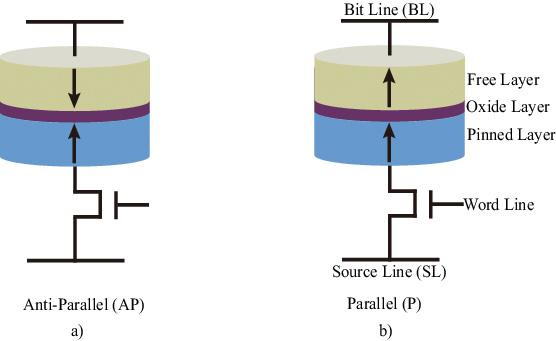
STT-MRAM cell structures. Image used courtesy of Zhang and co-authors.
The decision to integrate MRAM was equally driven by the need for a memory solution that could support increasingly software-driven automotive architectures. MRAM’s ability to act as both persistent storage and an extension of system memory provides automakers with new possibilities for managing real-time data structures within a zonal architecture.
Facilitating Zonal Architectures with Deterministic Communication
The S32K5 is designed to meet the increasing demand for high-bandwidth, low-latency communication in zonal architectures. It integrates a 2.5 Gbps 10Base-T1S Ethernet switch with MACsec security for high-speed data aggregation across vehicle domains.
The inclusion of a CAN accelerator further reduces system-level processing overhead by offloading CAN-to-Ethernet and CAN-to-CAN translation functions to dedicated hardware. This design effectively minimizes network stack complexity on the main processing cores and improves overall performance and reduces power consumption.
Zonal architectures also require MCUs that can efficiently manage real-time control while handling increasing software workloads. The S32K5 features a heterogeneous compute architecture, balancing Cortex-R52 and Cortex-M7 cores for compute and control tasks. A dedicated Cortex-M4 low-power engine, operating at 200 MHz, for efficient power management in standby modes.
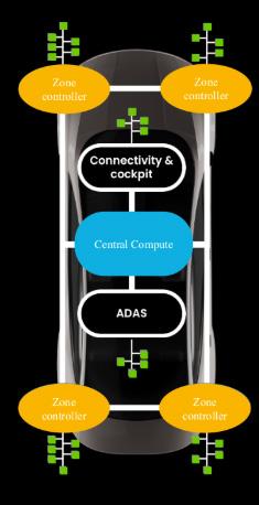
An automotive zonal architecture. Image used courtesy of NXP Semiconductors.
Finally, the architecture incorporates hardware-enforced isolation via NXP’s XRDC mechanism, allowing ECU functions to be segregated into independent execution domains. As Vieira explains, “We’ve implemented what we call XRDC—essentially a way to define independent compute or application domains in software but enforce them at the hardware level. You can isolate cores, memory, and even peripherals to ensure safety-critical applications don’t interfere with lower-priority tasks.”
This feature lets safety-critical applications run alongside lower-criticality functions without risk of interference. Independent core resets further enhance system reliability by allowing non-essential functions to be restarted without disrupting mission-critical operations.
Security and OTA Updates
The S32K5 integrates NXP’s latest security engine, which supports AES, ECC, SHA1/2/3, RSA, and PQC algorithms. These features mean that automotive ECUs can remain secure against evolving cybersecurity threats throughout the vehicle’s lifecycle. For example, the security engine facilitates trusted boot processes, secure key storage, and hardware-accelerated cryptographic functions, providing OEMs with a future-proof security framework.
Meanwhile, the combination of MRAM and an advanced security subsystem significantly enhances the reliability and speed of OTA updates. Traditional ECUs using embedded flash can require upwards of 45 minutes to complete an update, which inconveniences vehicle owners and presents operational challenges for OEMs.
The S32K5’s high-speed MRAM write capabilities, coupled with an optimized update process, enable firmware updates to be completed in seconds rather than minutes. This advancement improves the feasibility of frequent feature deployments and security patches, which aligns with the software-defined vehicle paradigm.
The ability to push updates rapidly and securely is also important for automakers seeking to monetize post-sale software features, enhance vehicle performance over time, and address emerging cybersecurity threats. By reducing the downtime associated with updates, NXP believes the S32K5 improves the overall vehicle ownership experience while enabling automakers to refine software-driven functionalities with minimal disruption.
A New Future for Automotive
With sampling set to begin in Q3 2025, NXP’s S32K5 microcontroller family represents an exciting step forward in the transition to zonal architectures and software-defined vehicles. By integrating MRAM, the MCU achieves a breakthrough in high-speed, low-latency OTA updates while eliminating the limitations of embedded flash.
The combination of deterministic networking, hardware-enforced isolation, and scalable compute capabilities enables automakers to build more modular, secure, and efficient vehicle architectures.
Looking to the future, Vieira says that the auto industry has evolved.
“Automakers aren’t just selling a vehicle anymore—they’re selling the next one to the same customer. That means vehicles need to improve over time, just like smartphones. The S32K5 helps make that possible by enabling secure, efficient, and scalable software updates throughout a car’s lifetime.”


