Last-Time Buy Notifications For Your ASICs? How To Make the Most of It
The semiconductor industry is continuously evolving, and while evolution is a good thing, it also means that some well-established technologies are inevitably approaching the end of their end of life. As those in the industry will know, many foundries have issued last-time buy notifications for their 600 nm ASICs as they pivot toward more efficient, smaller geometry nodes.

Last-time buy notifications for older ASICs create challenges and opportunities. Image used courtesy of Shutterstock (via EnSilica)
This will force companies in the automotive, aerospace, defense, telecommunications, and consumer electronics sectors to rethink their semiconductor designs. However, as we’ll discuss, that isn’t necessarily bad news.
Reviewing the Semiconductor Evolution
The journey of semiconductor technology has been marked by significant milestones. The 10 µm process developed in 1971 gave rise to the Intel 4004, which contained 2300 transistors and was the world’s first commercially produced microprocessor.
The pace of growth following this breakthrough was swift, with 6 µm and 3 µm processes following in 1974 and 1977, respectively. Each iteration improved on the last. By this time, Moore’s Law had been established. It predicted that chip density would almost double every two years as semiconductor technology advanced exponentially.
At the start of the 1980s, transistors were down to 1 µm in size, and companies were commonly packing more than 100,000 onto a chip. This number reached more than 1 million by the 1990s, and this is where the 600 nm process made its debut.
By now, the term “sub-micron” had become a reality, and the 600 nm process played a central role. This era saw the introduction of CMOS technologies that could integrate up to 4 million bits of SRAM and 16 million bits of DRAM—a substantial leap forward at the time. Notably, during this period, Intel transitioned from the 486 processor, which utilized 600 nm technology, to the first generation of Pentium processors, which used a more advanced 350 nm process.
During the 600 nm era, 8-inch (200 mm) wafers became the industry standard, and 5 V logic levels were commonly used. This period also saw the development of various process variants, including BiCMOS and BCD technologies, which enabled mixed-signal applications that featured analog and digital signals. These innovations allowed products developed on 600 nm processes to remain in production for many years, used in everything from consumer electronics to industrial equipment.
The Transitions to Low Voltage and 300 mm Wafers
Despite the impressive capabilities of the 600 nm process, the relentless pace of Moore's Law drove the industry towards smaller geometries, greater logic density, and larger wafers. The introduction of 12-inch (300 mm) wafers and the shift to lower logic voltages, such as 3.3 V, marked the beginning of a new chapter.
Foundries initially maintained dual production lines for 200 mm and 300 mm wafers, but technological advances like copper metallization and shallow trench isolation (STI) made it increasingly challenging to sustain both profitably.
This evolution has led to the current situation. Many foundries are issuing last-time buy notifications for their classic 600 nm processes, prompting manufacturers to consider migrating to newer technologies.
Last-Time Buy Notifications—Why Now?
As semiconductor processes have evolved from 600 nm to smaller geometries, materials used in older technologies have become harder to source and often no longer meet current environmental and safety regulations. Maintaining equipment for these outdated processes has also become increasingly costly, making it unsustainable for foundries to continue their production.

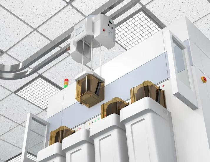
Increased automation is a key driver of manufacturing efficiency improvement for modern semiconductor processing. Image used courtesy of Adobe
The significant advantages of newer processes have also become too good to ignore. Processes like 130 nm and 180 nm support higher logic density, improved power efficiency, and enhanced reliability with features such as copper metallization and shallow trench isolation (STI). The transition to 12-inch (300 mm) wafers has further solidified these newer processes as industry standards, providing better performance and cost-effectiveness for modern applications.
Problem or Opportunity?
While the initial response to last-time buy notifications may be a concern over the cost and complexity of migrating designs, this should be seen as an opportunity rather than a business-halting problem to overcome. Higher performance, lower power consumption, and increased functionality become far more accessible.
Foundries like GlobalFoundries (GF), Taiwan Semiconductor Manufacturing Company (TSMC), XFAB, and SK keyfoundry offer extensive options to facilitate migration from 600 nm. This ensures a stable supply chain while opening up avenues for product improvement and innovation.

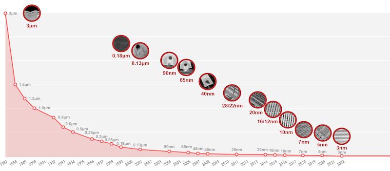
TSMC’s silicon technologies through the years. Image used courtesy of TSMC
This migration to modern processes will be crucial for industries such as automotive manufacturing, where industry standards are heavily enforced, and a reliable supply chain is essential to production.
The Benefits of Design Migration
Let’s start with the benefits. Migrating designs from 600 nm or 350 nm to more modern processes like 180 nm or 130 nm offers numerous advantages:
- Newer technologies provide higher logic density, allowing for more functionality within the same silicon area.
- More complex and powerful circuits can be integrated, enhancing overall product capabilities.
- Advanced nodes can support higher clock frequencies or lower power consumption, depending on their design requirements.
- Copper BEOL metallization and up to eight metal layers improve resilience to electromigration and offer better performance for high-speed signals.
- Shallow trench isolation (STI) technology enhances density and reduces the risk of “latch-up,” a common point of failure in older processes.
Compatibility with 5 V Systems
Compatibility with existing designs, however, should be a key consideration. Many newer processes offer dual gate oxide options, maintaining compatibility with older 5 V I/O standards while providing the benefits of more modern technologies. This ensures that designs can be updated with minimal changes to their original specifications.
Increased Device Options
What’s more, 130 nm BCD nodes are now very mature technologies that offer many more process options, including different high voltage classes of transistors, non-volatile memories (OTP, flash), MIM caps, Zener or Schottky diodes, etc. This can benefit the integration of complex analog/RF functions into more competitive system-on-chip solutions. Higher levels of integration provide options for trimming on-chip analog functions and calibration of external sensors, offering system-level cost benefits.
Improved Functionality and Yield
The smaller feature size of 130 nm allows the integration of Arm Cortex-M class processors (or similar RISC-V) with little extra silicon cost. Indeed, the required CPU performance and memory requirement will be the dominating factors in the viability of integration. Low-end CPUs require just a couple of square millimeters of silicon area. Similarly, 64 or 128 Kb of SRAM can be integrated cost-effectively.
The availability of a wide range of silicon-proven third-party IP, both analog and digital, simplifies the integration of additional functionality that simply wasn’t possible with 600 nm processes. Further, the improved lithography used for the newer 12-inch wafers offers improved defect rates and better device matching for improved manufacturing yield.

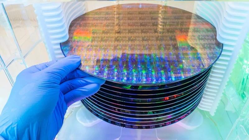
Modern wafer processes reduce human handling to improve yield. Image used courtesy of Adobe
Practical Steps and Timescales
The migration of a 600 nm or 350 nm CMOS product to a 130 nm process involves several key steps and considerations, typically starting with a thorough assessment of whether the new design will be pin-to-pin compatible with the old one or if it should include new functionality.
This decision significantly impacts the engineering effort required. For instance, a full re-design might be necessary due to the age and potential obsolescence of the original design databases. This will involve planning and technology selection, design, simulation, and validation.
It’s also worth noting that, depending on the complexity, design efforts can take several months. Then, another three or more months for manufacturing and additional time for validation and qualification. Put simply, the existence of legacy design databases does not guarantee an automatic migration of the design.
Reasons To Be Optimistic
Migrating to a newer process technology like 130 nm ensures continuity and offers opportunities to enhance and modernize. For instance, automotive safety standards such as ISO 26262, which were not available during the 600 nm era, can be seamlessly integrated into the new design without significantly increasing the silicon area.
Newer technologies also support higher integration levels, allowing for additional capabilities like integrated sensors and enhanced communication interfaces. This can significantly alter the value and use cases associated with various products.
Then, of course, there are benefits to leveraging a modern supply chain. Most 300 mm wafer fabs already offer certain certifications, which can contribute to a smoother production process. This is particularly beneficial for industries that require long-term supply commitments, such as aerospace and automotive.
In that sense, it’s a win-win! Redesigning an older aerospace component to a newer technology can reduce costs and improve performance while at the same time meeting stringent qualification requirements. This can transform a legacy product into a more competitive and future-proofed solution, opening up new market opportunities and extending its lifecycle.
So, the last-time buy notification is nothing to be feared; it’s simply innovation in action. With the right mindset and some careful planning, it will raise the bar for all.


