How To Withstand Electrical Stresses in Modern Op Amps
In some operational amplifier (op amp) designs, it isn’t possible to avoid the presence of an input voltage when the supply rail needs to be off. This is usually because a sensor or other input is on a different power supply than the amplifier when the amplifier is shut off.
The amplifier will have internal protection structures for resistance against electrostatic discharge (ESD) during manufacturing, but these structures are not intended to protect the amplifier from more extreme conditions such as an electrical overstress (EOS) event. There are some design modifications and basic design principles that can help mitigate the possibility of damage to the op amp.
Protection Structures in Modern Op Amps
First, let’s talk about the existing protection structures present in most modern op amps. Some data sheets will include diagrams of the protection structures. Figure 1 is from the data sheet of the OPA2991 from Texas Instruments (TI).
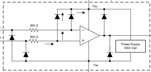
Figure 1. A diagram of an op amp equivalent internal ESD structure
Amplifier protection structures usually have diodes on the input pins connected to the drain supply voltage (VDD) and the source supply voltage (VSS), and the output will also have diodes to VDD and VSS, which are inherent to the amplifier output stage. A class AB amplifier output stage will have output transistors connected to each rail, and each output transistor has an inherent P-N junction that acts as a diode to either VDD or VSS.
Since these body diodes are “free,” there is no need to add another ESD cell, as the output transistor body diodes are usually larger and end up being more capable of withstanding ESD strikes than a discrete ESD diode.
Op amps that do not have input ESD diodes to both VDD and VSS are generally promoted as a benefit for specialized functions; for example, the TI OPA310 has fail-safe inputs. The fail-safe inputs are a specialized diode structure that allows input voltage to be present when the device is unpowered, up to a certain point.
The input diodes are present to steer large voltage spikes of either polarity to the power rails so that the ESD cell can dissipate the energy to ground in a controlled way. The ESD cell is inactive in normal operation, and will usually either be magnitude- or edge-triggered.
Magnitude-triggered ESD cells turn on when a large-enough magnitude spike is present. Edge-triggered ESD cells turn on when applying a fast-enough rising or falling edge to the input. Since ESD spikes are generally in the magnitude of hundreds or thousands of volts or more and have durations less than 100 ns, the activation point is set well beyond the normal operational expectations of the op amp to avoid sinking excess current or latching on when a simple, small overvoltage is present.
Diodes Connected Back-to-Back
In some cases, there are diodes connected back to back between the inputs of the op amp that keep the input differential pair from seeing a large difference in the voltage. These diodes are not implemented for ESD protection, and are primarily designed to protect the input differential pair.
As shown in Figure 2, they will usually have a higher forward voltage so that they do not trigger during the normal operation of the op amp. You don’t usually have to consider these diodes for EOS protection, since there are other conduction paths with lower forward voltages, but it is important to consider them for EOS analysis when you expect a large input-voltage differential.
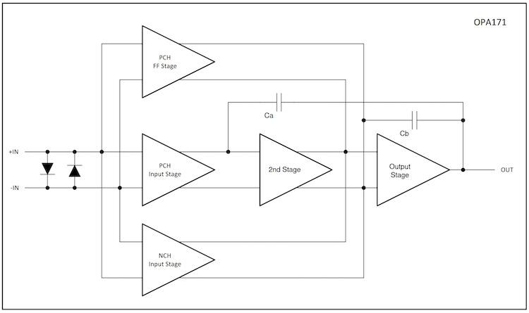
Figure 2. OPA171’s functional block diagram illustrating the back-to-back input diodes
These back-to-back input diodes were necessary in op amps because a large input-voltage differential would damage the input transistors. In TI’s multiplexer-friendly input amplifiers, there are no back-to-back input diodes, and a different structure protects the input differential pair from the application of a large input-voltage differential. In multiplexer-friendly amplifiers, you do not need to consider back-to-back diodes between the inputs as a valid conduction path.
Let’s take a look at several different EOS protection structures, and when these structures may be applicable to your design.
The “Most Protection” Approach
When the function of the amplifier is a priority and the potential overstresses are somewhat unknown, it is necessary to control the potential for EOS at all of the pins going into the op amp. Figure 3 shows a method to protect the inputs, outputs and supply pins of a single-channel op amp.
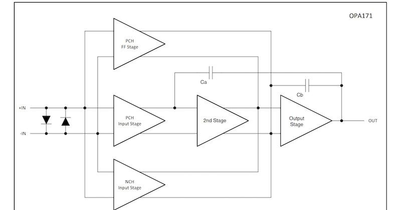
Figure 3. An op amp design with overvoltage protection on the input pins, output pins and supply pins. (Click image to enlarge)
The implementation in Figure 3 offers the most comprehensive protection for your op amp, and you can use it in most applications with no issues. It is the most expensive option, however, both in terms of printed circuit board area and cost. On the input pins, external diodes connected to the op-amp supply rails before resistors will ensure that an overvoltage condition will flow through the external diodes and not through the op amp’s internal diodes.
This is because the voltage drop across R2 and R1 ensures a larger voltage on diodes D1 and D2 instead of the amplifier’s input ESD diodes. The external protection diodes must have an appropriate current rating, and should be able to sink the current that can be generated before the op amp inputs.
The example in Figure 3 includes the BAV99 as a common diode for EOS protection. The output follows a similar convention, with the diodes and resistors placed to ensure that the external diodes conduct first before the output stage diodes. This is especially important on the output stage, as the output diodes will typically have a lower forward voltage than most external protection diodes.
Secondary Purpose
These resistors serve a secondary purpose as well. The protection diodes have parasitic capacitance, and placing a resistor between the feedback loop and the diode will keep the diodes’ parasitic capacitance from loading the feedback loop, and maintain loop stability.
At the supply rails, Zener diodes will help protect against an overvoltage on either supply pin, and provide a low-impedance path to ground when a potential overvoltage event is present. The op amp remains protected from overvoltage regardless of the VDD and VSS rail’s ability to sink or source current.
It’s worth noting that even in this configuration, there can be some unintentional effects. If the op amp must source or sink current, there will be some voltage inaccuracy on the OUT node. Implementing the isolation resistor (RISO) with a dual feedback circuit can overcome this voltage drop.
If the supply rail is high impedance when turned off, and the circuit is relying on the Zener diodes to clamp the op amp voltage, it is possible for the op amp to self-power through the protection diodes. Whatever IC follows the amplifier must be able to tolerate a voltage being present on the output of the op amp.
The Acceptable Approach
The acceptable approach will help mitigate EOS events, but since there are internal diodes in the amplifier, it’s important to leverage them carefully to prevent damage to the op amp. In the TI OPA992, OPA2992 and OPA4992 op amp data sheet, the absolute maximum ratings table (Figure 4) includes what input currents are considered safe.
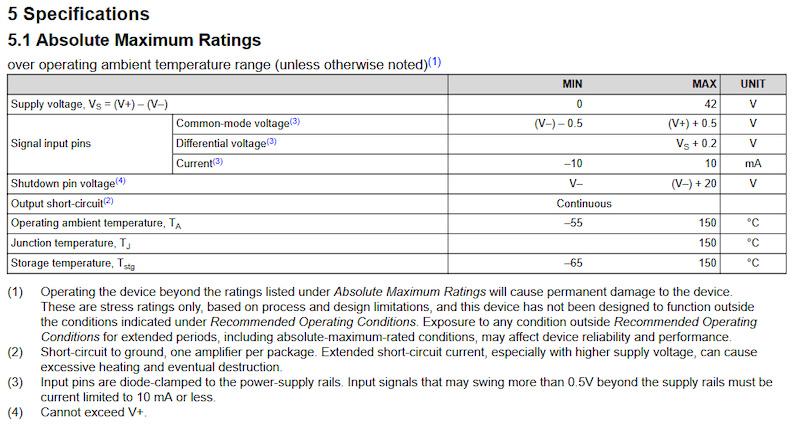
Figure 4. An excerpt from the OPA992, OPA2992 and OPA4992 absolute maximum ratings table. (Click image to enlarge)
The data sheet specifies that the input voltage must be limited to within 0.5 V of V+ or V–, and must not exceed 10 mA sinking or sourcing. Additionally, the supply voltage must not exceed 42 V of potential difference between the two supply pins.
Let’s look at two potential protection scheme scenarios. In scenario No. 1, supplies can source and sink current, and the input overvoltage condition is a known voltage (Figure 5).
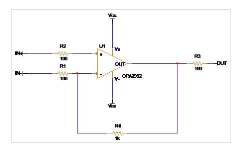
Figure 5. An op amp with simple series resistor EOS protection
In Figure 5, the minimum protection necessary to protect the amplifier is to limit the input current to less than 10 mA. With 100 Ω series input resistors, the maximum overvoltage condition that can be mitigated at inputs IN+ and IN– is 1 V above or below the supply rail. If the overvoltage condition is going to be a sustained event—for example, a sensor providing an input voltage when the supplies are turned off—then you will want to further limit the current.
Reducing the stress condition below the maximum allowable condition is similar in concept to capacitor voltage derating, where operating well below the limit will put less stress on the system than operating at the limit. For an absolute maximum input current of 10 mA, limiting the input current to less than 1 mA will help further mitigate the potential for damage in the case of a sustained overvoltage event.
Scenario Number 2
In scenario No. 2, the overvoltage condition is a known voltage, and supplies are high Z; for example, there is a low-voltage amplifier that must be resilient to a short-to-12V battery voltage (VBAT) condition on the input (Figure 6).
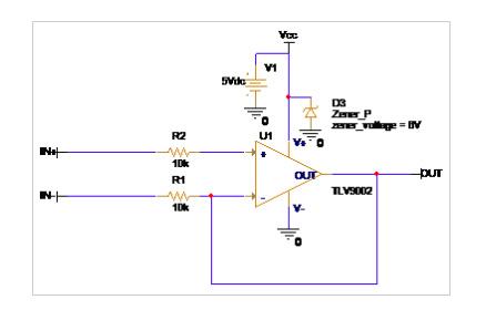
Figure 6. An op amp with series resistor input protection with an added Zener diode on the supply rail
With a supply voltage of 5 V, the difference between a 12 V short condition and the 5 V amplifier supply is 7 V. To keep this short condition from sourcing more than 10 mA into the amplifier, you need 700 Ω on the input of the amplifier. And to keep this current under 1 mA, you need 7 kΩ. Adding a standard and common resistor value, placing a 10 kΩ series resistor on the input of the amplifier should limit the current to a safe level. To confirm that this series resistor will protect the op amp, see the absolute maximum ratings of the TI TLV9002, shown in Figure 7.
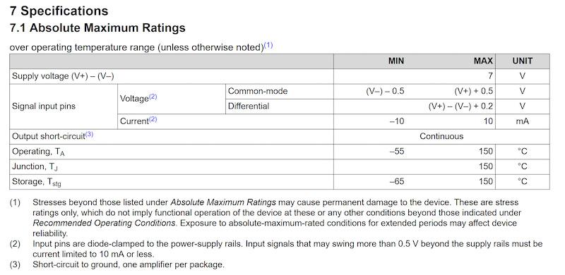
Figure 7. Excerpt from the absolute maximum ratings table for the TLV9002 op amp. (Click image to enlarge)
Adding a Zener diode from VCC to ground, with a reverse voltage of 6 V, will keep the op amp supply pin from exceeding a supply voltage above the absolute maximum rating of 7 V. In cases where the supply can source and sink current, the supply rail will be able to properly regulate and protect the supply voltage of the amplifier without the need for a Zener diode.
You must also consider the input voltage, which is limited between (V–) –0.5 V and (V+) +0.5 V. A short-to-12V VBAT condition does violate the input-voltage limitation; however, there is a footnote in Figure 7 that specifies that if the input signal is outside the supply rails, it must be limited to 10 mA or less. The ability to meet this condition greatly reduces the likelihood of damage and does not violate the ratings in the absolute maximum table.
Figure 8 summarizes these design requirements.
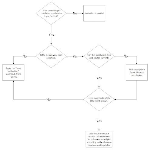
Figure 8. A flow chart for which EOS protection scheme is relevant to your application. (Click image to enlarge)
All About Preventing Damage
In amplifier circuit design, it can be an unavoidable circumstance to have an overvoltage event at the amplifier. The resources in this article should equip you with multiple options that fit various cost restrictions, as well as internal IC limitations to help prevent damage to the IC when an overvoltage event occurs. In future designs, these guidelines can help you build circuits that can withstand these events without damage.
Additional resources
Watch the TI training video, “Op Amp Stability,” to learn more about the RISO implementation with a dual feedback circuit.