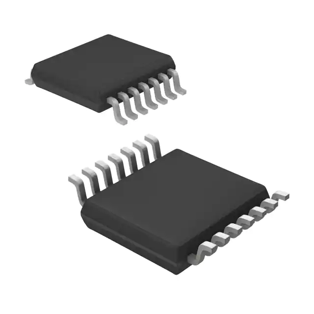
Overview
The CD74HC4094PWR-E, produced by Texas Instruments, is a high-speed CMOS logic 8-stage serial shift and store bus register. This device features a storage latch associated with each stage, allowing for the transfer of data from the serial input to parallel buffered tri-state outputs. The parallel outputs can be connected directly to common bus lines, making it versatile for various applications. Data is shifted on positive clock transitions, and the data in each shift register stage is transferred to the storage register when the Strobe input is high. The output appears whenever the Output-Enable signal is high.
Key Specifications
| Parameter | Symbol | Value | Units |
|---|---|---|---|
| Operating Voltage Range (HC Types) | VCC | 2 to 6 | V |
| Operating Voltage Range (HCT Types) | VCC | 4.5 to 5.5 | V |
| Maximum CP Frequency | fMAX | 30 MHz (HC), 24 MHz (HCT) | MHz |
| Input Capacitance | CIN | 10 | pF |
| Power Dissipation Capacitance | CPD | 90 pF (typical) | pF |
| Tri-state Output Capacitance | CO | 15 | pF |
| Propagation Delay Time (CP to QS1) | tPLH, tPHL | 16 ns (typical) | ns |
| Output Transition Time | tTLH, tTHL | 15 ns (typical) | ns |
| Operating Temperature Range | Tj | -55°C to 125°C | °C |
| Fanout (Standard Outputs) | 10 LSTTL loads | ||
| Fanout (Bus Driver Outputs) | 15 LSTTL loads |
Key Features
- Buffered Inputs: Ensures stable input signals.
- Separate Serial Outputs: Synchronous to both positive and negative clock edges for cascading.
- Wide Operating Temperature Range: From -55°C to 125°C.
- Balanced Propagation Delay and Transition Times: Enhances signal integrity.
- Significant Power Reduction: Compared to LSTTL logic ICs.
- High Noise Immunity: NIL = 30%, NIH = 30% of VCC at VCC = 5 V for HC types.
- Direct LSTTL Input Logic Compatibility: For HCT types, VIL = 0.8 V (Max), VIH = 2 V (Min).
- CMOS Input Compatibility: Il ≤ 1μA at VOL, VOH.
Applications
- Serial to Parallel Data Conversion: Useful in systems requiring serial data to be converted into parallel format.
- Cascaded Systems: The separate serial outputs allow for easy cascading of multiple devices.
- Bus Systems: The tri-state outputs can be connected directly to common bus lines.
- High-Speed Data Processing: Suitable for applications requiring high-speed data shifting and storage.
- Industrial and Automotive Systems: Given its wide operating temperature range, it is suitable for harsh environment applications.
Q & A
- What is the primary function of the CD74HC4094PWR-E?
The primary function is to act as an 8-stage serial shift and store bus register, converting serial data to parallel format.
- What are the operating voltage ranges for HC and HCT types?
HC types operate from 2 to 6 V, while HCT types operate from 4.5 to 5.5 V.
- What is the maximum clock frequency for the CD74HC4094PWR-E?
The maximum clock frequency is 30 MHz for HC types and 24 MHz for HCT types.
- How many LSTTL loads can the standard outputs drive?
The standard outputs can drive up to 10 LSTTL loads.
- What is the operating temperature range of the CD74HC4094PWR-E?
The operating temperature range is from -55°C to 125°C.
- Does the CD74HC4094PWR-E have high noise immunity?
Yes, it has high noise immunity with NIL = 30%, NIH = 30% of VCC at VCC = 5 V for HC types.
- Can the CD74HC4094PWR-E be used in cascaded systems?
Yes, it can be used in cascaded systems due to its separate serial outputs synchronous to both positive and negative clock edges.
- What is the input capacitance of the CD74HC4094PWR-E?
The input capacitance is 10 pF.
- Is the CD74HC4094PWR-E RoHS compliant?
Yes, the CD74HC4094PWR-E is RoHS compliant.
- What are the typical propagation delay times for the CD74HC4094PWR-E?
The typical propagation delay times are around 16 ns for CP to QS1.


