OmniVision Delivers Compact, High-Performance 50 Megapixel Camera Chip
OmniVision has released the OV50M40 image sensor, packing 50-megapixel resolution, high dynamic range (HDR) video, and low power consumption into a 1/2.88 inch lens CMOS sensor. The new sensor is optimized for small size to better fit into front- or rear-facing smartphone cameras without compromising performance.
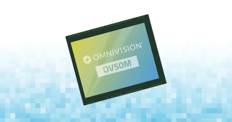
OmniVision OV50M sensor.
The sensor uses a stacked die to increase processing power without expanding the silicon die size. On-sensor processing allows it to deliver staggered high dynamic range (HDR) and dual analog gain (DAG) HDR. Low power drain enables always-on operations such as motion activation.
Key Specifications of the OV50M40
The CMOS sensor features 0.61 µm square pixels at a maximum resolution of 8192 x 6144 (50 MP). At full resolution, it transfers at 12 frames per second. Preview and video resolution is 4096 x 3072 pixels (12.5 MP) and 60 frames per second transfer. The high pixel count gives the sensor fast switching between full resolution and 2x or 3x digital crop-zoom resolutions. It also offers fours-pixel binning to increase light sensitivity.
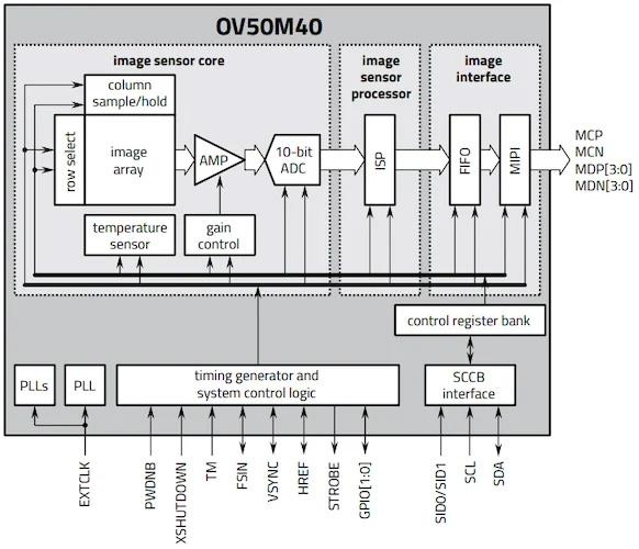
OV50M40 functional block diagram.
The sensor has a maximum lens size of 1/2.88” and supports various output formats, including 10-bit RAW, 12/14-bit for HDR, and 8-bit RGB RAW for ultra-low power (ULP) mode. The device has a 1.1-V core, 2.8-V analog section, and 1.8-V or 1.2-V I/O. Active power draw is 346 mW at 50 MP and 366 mW at 12.5 MP, and standby power is less than 30 µA. The OV50M40 also supports video formats ranging from 4K/2K with PDAF autofocus at 60 fps to 1080P at 120 fps.
More Processing on the Sensor
OmniVision based the new sensor on its PureCel Plus‑S stacked-die technology. The system better utilizes available space in the sensor chip. Most CMOS sensors have an inert chip carrier wafer under the sensor. The carrier adds strength and stability to the chip. This conventional architecture puts processing electronics on the same active wafer as the light-detecting area. Doing so utilizes space that could otherwise be dedicated to light gathering. The OmniVision PureCel Plus‑S sensor replaces the non-active carrier with an active silicon wafer containing analog and digital processing electronics. This frees up more surface area for the sensor and provides more area for advanced on-sensor processing without increasing the overall chip size.
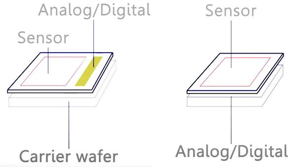
Conventional sensor architecture on the left and Plus-S stacked architecture on the right.
The larger active area is used for on-sensor noise reduction, improving dynamic range, reducing autofocus time, and other image quality-related functionality. One of the key features that has been implemented, taking advantage of the improved space and pixel use, is single exposure dual analog gain (DAG) video HDR. In single-exposure dual analog gain sensors, two pixels are engaged simultaneously. One is amplified when it detects the low-brightness end of the capture range, and the other captures the high-brightness end of the range. Using analog comparison on the two pixels captures high dynamic range in a single frame at up to 4K video resolution.
Greater Sensitivity
The PureCel Plus‑S technology in the sensor helps to deliver better low-light image quality and decreases power consumption in a smaller form factor. Typically, a smaller size means a lower ratio of light-capturing area to support circuitry. However, OmniVision used a smaller CMOS process node to reduce the size of the circuitry, leaving more space for the light capture area.
The company also reduced the overall chip stack height with buried color filters. In deep trench architecture, the light-sensitive area is down in the silicon. Color filters and microlenses are stacked on top. The disadvantage is that this setup narrows the possible field of view for the sensor. By dropping the filters down in the OV50M40, the stack height is reduced, and the field of view and accompanying light-gathering capability is increased, allowing the sensor to be implemented in even thinner devices. OmniVision also uses composite metal grid deep trench isolation (DTI) to minimize light crossover from one pixel to the next. When combined with on-sensor electronics, the DTI contributes to lower noise and, thus, better low-light sensitivity.
The new sensor is available in sample quantities and is planned for production volumes in Q4 2024.

