IBM Introduces Co-Packaged Optics, an Optical Link Packaging Scheme
IBM Research recently announced a new co-packaged optics technology, an innovation to address modern data centers' bandwidth and energy challenges.
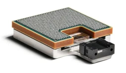
IBM’s prototype polymer optical waveguide solution. Image used courtesy of IBM
As data centers struggle to scale with the increasing demands of large language models and other AI applications, traditional copper-based interconnects are reaching their limits in bandwidth and energy efficiency. The resultant bottleneck has become a significant hindrance to performance and efficiency, especially in AI and cloud computing. By transitioning to optical solutions, IBM hopes its co-packaged optics will bypass these limitations and pave the way for the next generation of AI-driven infrastructure.
IBM Unveils Co-Packaged Optics Tech
IBM designed its new co-packaged optics technology to improve data center energy efficiency and bandwidth, particularly for generative AI computing.
To do this, the research team integrated optical link connections directly onto circuit boards and chips utilizing polymer optical waveguides to achieve high beachfront density. The polymer waveguides support a 50-micron pitch for optical channels—an 80% reduction compared to traditional 250-micron pitch designs. As a result, the systems achieved a 1,000% to 1,200% increase in bandwidth capacity. Importantly, the optical fibers, measuring 250 microns in diameter, maintained alignment tolerances of under half a micron to guarantee high-fidelity connections.
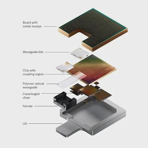
The prototype co-packaged optics module. Image used courtesy of IBM
IBM also claims that the technology delivers significant energy efficiency improvements, reducing energy consumption by 80% from five picojoules per bit to under one picojoule per bit. Meanwhile, the photonic integrated circuit (PIC) connections achieved insertion losses below 1.2 dB per channel, outperforming the standard 1.5-2-dB range, while cross-talk remained under 30 dB. The waveguides also support multi-wavelength data transmission, potentially increasing bandwidth by up to 8,000%.
Integration Challenges for Optical Systems
Integrating optical systems into chip and circuit board designs historically has been a notable technical challenge due to the competing requirements for precision, scalability, and compatibility with existing manufacturing processes. While optical data transmission offers substantial advantages in bandwidth and energy efficiency compared to traditional electrical interconnects, its implementation is constrained by factors such as alignment tolerances, material compatibility, and thermal stability.
Generally, it is difficult to achieve precise alignment between optical fibers and silicon photonics waveguides. High-fidelity optical connections require sub-micron tolerances, typically within 0.5 microns, to minimize insertion loss and maintain signal integrity. Misalignments can increase insertion loss beyond acceptable thresholds, leading to degraded performance. For example, insertion losses in conventional optical systems range between 1.5 dB and 2 dB per channel.
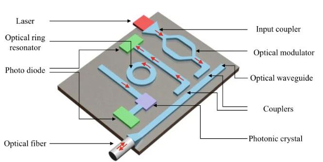
An example photonic integrated circuit. Image used courtesy of Ovaga
Thermal stability is another obstacle since optical components must maintain consistent performance across wide temperature ranges. Temperature variations can induce mechanical stress and refractive index changes, disrupting signal transmission. Materials such as polymers and glass must be carefully engineered to withstand these fluctuations without compromising optical properties.
Finally, scalability is a hurdle. The diameter of a single optical fiber limits how densely connections can be packed at the edge of a chip. Reducing the pitch of optical channels, as IBM achieved with its 50-micron design, increases density but requires innovations in waveguide fabrication and packaging. Integrating these compact designs with existing semiconductor manufacturing processes adds another layer of complexity.
Lighting the Path to Computing Efficiency
IBM’s co-packaged optics technology provides a glimpse into how data centers can evolve to meet the unprecedented demands of generative AI and other high-performance computing workloads. By addressing fundamental bottlenecks in bandwidth and energy efficiency, this solution may lay the groundwork for more sustainable and scalable AI infrastructure. While the technology is currently in the prototype stage, IBM is working with suppliers and scaling production. This suggests that co-packaged optics may soon transition from research to real-world deployment.

