IBM Boasts Industry-Leading Photonics to Cut AI Training Speed
IBM said this week that the company leads the semiconductor industry with the development of a silicon photonics technology that could speed data center training by as much as 5×.
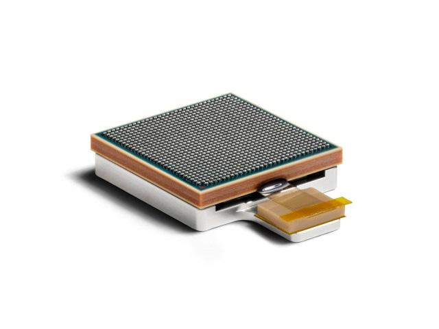
IBM’s co-packaged optics (CPO) enable connectivity in data centers to complement existing short-reach electrical wires. The company designed and assembled what it calls the first successful polymer optical waveguide (PWG) behind the technology.
IBM said the tech will also cut costs for scaling generative AI by reducing power consumption compared with mid-range electrical interconnects, while extending the length of data center cables. As new data center projects are announced almost daily, they will consume 8% of U.S. power by 2030, compared with 3% in 2022, according to a Goldman Sachs report published in May.
“We see this as the leading technology and well ahead of anyone,” John Knickerbocker, an BM distinguished researcher, told reporters. “It’s ready from a technology perspective to be scaled into manufacturing. We built it in our manufacturing site in Bromont, [Canada], where they have both piloting as well as manufacturing operations.”
IBM plans to license the tech to chip foundries for commercial production.
“We do need to share design manuals and PDKs associated with this co-packaged, optics technology with manufacturers,” IBM VP Mukesh Khare said at an event. IBM will work with chip designers to develop silicon photonics products, he added.

IBM optics module 2 (Source: IBM)
IBM will compete with companies like GlobalFoundries and Tower Semiconductor, which have been among the leaders in silicon photonics.
Bringing optical connections onto circuit boards and all the way to chips results in a more than 80% reduction in energy consumption compared with electrical connections, Knickerbocker found—a reduction from 5 picojoules per bit to less than 1.
GlobalFoundries says its customers have already demonstrated 5 picojoules per bit on silicon. The company expects to go below 5 picojoules in the next generation of its silicon photonics process.
IBM says its tech offers size advantages.
“The research demonstrations that we’ve seen in the technical literature show people getting down to about a 50-micron pitch,” Knickerbocker said. “We’re down at an 18-micron pitch for these optical waveguides.”
By using optical waveguide technology, IBM has put as many as 6× more optical fibers at the edge of a silicon photonics chip compared to what was possible before, Khare said. That will translate into as much as 80× improvement in bandwidth between chips, he added.
“If you have if you have 10,000 accelerators in a data center, you need to be able to talk to accelerators which are a few meters apart, not just a few inches apart,” Khare said. The IBM technology can achieve 100 meters at high bandwidth..
IBM aims with its waveguide tech to outmode the glass fiber that is currently used for interconnect.
Glass fiber is rather large, on the order of 250 micron, or about three diameters of a human hair, allowing only four connections per millimeter on the edge of a chip compared to the 51 that IBM announced with the new technology.
“We designed the optical waveguides, and we designed the package that it sits on,” Knickerbocker said. It took years and many iterations of learning and enhancement to optimize the materials which were custom made for IBM, he added.
Adiabatic coupling
One of the key technologies that IBM used, called adiabatic coupling, improves the interface between chip and optics.
“If you’ve got a chip and the polymer waveguide, they sit just overlapping so slightly,” Knickerbocker said. “It allows the light—without touching—to jump from the polymer waveguide into the chip or from the chip back into the waveguide by having a very thin, fine line. You basically are transitioning the light that’s in the channel from the polymer waveguide into a light channel on the chip. That’s also a waveguide, but of a different material. Adiabatic coupling allows you to do so with almost no loss, very little loss. It’s a great technology, very robust.”
IBM said its CPO technology opens a new pathway to meet AI’s increasing performance demands, with the potential to replace off-module communications from electrical to optical.
Although IBM does not make chips, the latest development continues IBM’s leadership in semiconductor innovation, including the world’s first 2-nm chip technology, the first implementation of 7-nm and 5-nm process technologies, nanosheet transistors, and vertical transistors.


