Broadcom Reaches New Processing Heights With Stacked Die and Face-to-Face Chiplets
Broadcom recently introduced its latest in high-capacity chip packaging, the 3.5D eXtreme Dimension System in Package (XDSiP) platform. The platform technology builds on up to 6,000 mm2 of silicon distributed between up to 12 high-bandwidth memory (HBM) stacks, multiple 3.5D integrated accelerator chiplets, and high-speed interposer circuitry.
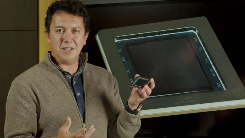
Frank Ostojic, Broadcom's general manager of ASIC products, with a 3.5D XDSiP custom accelerator chip.
A high-density, face-to-face connection architecture doubles the processor core area. According to Broadcom, this increased density and performance may accommodate the next generation of custom accelerator processing units (XPUs) used in AI data centers.
Benefits of 3.5D XDSiP Packaging
In the diagram below, the processing unit chiplets of the XDSiP platform are depicted in red.
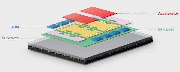
Rendering of XPU utilizing XDSiP platform architecture.
These can be any ultra-high-performance accelerators such as graphic processing units (GPUs), tensor processing units (TPUs), or application-specific integrated circuits (ASICs). The yellow base die chiplets can contain more processing circuitry, SRAM, network interconnect (NIC), or other custom circuitry. The accelerator and base die are connected face to face. The HBM stacks (in blue) surround the processing chiplets. Conventional 2.5D looks very similar to this but does not have the stacked accelerator chiplets.
Some of the key benefits of this 3.5D XDSiP packaging includes:
- Up to double the processing chiplet area for the same overall chip package size
- 7x increase in interconnect signal density between stacked dies over F2B systems
- 10x reduction in die-to-die power consumption with HCB
- Allows mixing of different processor nodes
- Reduced signal latency between functional blocks
- Reduced interpose size, which saves raw materials and increases yields
Defining a Few Terms Behind 3.5D XDSiP
2.5D processor design refers to the process of splitting functionality among multiple silicon chiplets and placing these chiplets on an interposer. The interposer acts as the substrate and high-speed interconnect between chiplets. 2.5D allows easy integration of multiple different processor cores, specialized circuitry, and memory all in one package—often called a system in package (SiP).
3D silicon stacking is somewhat self-evident. Chiplets are stacked one on top of the other. 3D HBM is typically available in stacks of 2, 4, 8, or more memory chiplets. More recently, companies have started stacking processor and application-specific chiplets on top of each other. While 3D architecture can significantly increase density, it also increases the risk of thermal issues.
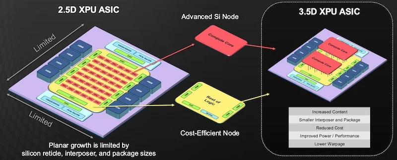
The move to a 3.5D XPU ASIC affords computing performance growth.
Broadcom's approach utilizes both design and software to ensure thermal performance. The “3.5D” architecture combines 2.5D chiplet structure with 3D stacked die and a face-to-face (F2F) processor core interconnect configuration. With F2F, the most critical chiplets are stacked with their top sides facing each other. One die will be oriented right side up and the next in the stack up will be upside down. This arrangement enables shorter interconnect distances and faster data transfer with fewer artifacts. Interconnects can be improved by placing the chiplets facing each other and using hybrid copper-to-copper bonding (HCB). Copper pillars extend from each face to directly connect.
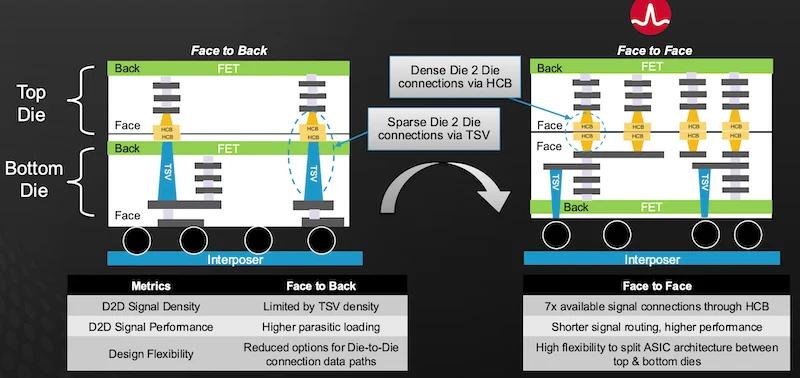
Face-to-back vs. face-to-face structure.
The legacy alternative, face-to-back (F2B), stacks all chiplets in the same orientation. F2B inter-chiplet connections are made with through-silicon vias. By combining 2.5 chiplet architecture, 3D stacked chiplets, and F2F, Broadcom has developed what they consider to be the highest-performing large-chip architecture.
Moore’s Law Extends Into Three Dimensions
Generative AI is taxing conventional system-in-package (SiP) processor architecture. AI training requires clusters of 100,000 or more processing units, with some installations nearing or exceeding one million XPUs. As the silicon geometries shrink to near the minimum practical, architectural changes are needed to improve AI processing density.
Gordon Moore may have been thinking only about two-dimensional silicon etching when he coined his law, but that doesn’t mean that the industry can’t keep it going by thinking in 3D. The Broadcom 3.5D XDSiP is designed to do just that and keep the law in force. The system is compatible with fab processes from TSMC and has been fabbed for a proof-of-concept demonstration.