


Overview
The CD74HCT4094M96 is a high-speed CMOS logic 8-stage serial shift register produced by Texas Instruments. This device features a storage latch associated with each stage, allowing for the transfer of data from the serial input to parallel buffered tri-state outputs. The parallel outputs can be connected directly to common bus lines, making it versatile for various applications. Data is shifted on positive clock transitions, and the data in each shift register stage is transferred to the storage register when the Strobe input is high. The Output-Enable signal controls the appearance of data at the outputs.
Key Specifications
| Parameter | Value | Unit | Conditions |
|---|---|---|---|
| VCC (Supply Voltage) | 4.5 to 5.5 | V | |
| VIL (Low-level Input Voltage) | 0.8 | V | At VCC = 5 V |
| VIH (High-level Input Voltage) | 2 | V | At VCC = 5 V |
| VOH (High-level Output Voltage) - CMOS loads | 4.4 | V | IOH = –20 μA |
| VOH (High-level Output Voltage) - TTL loads | 3.98 | V | IOH = –6 mA |
| VOL (Low-level Output Voltage) - CMOS loads | 0.1 | V | IOL = 20 μA |
| VOL (Low-level Output Voltage) - TTL loads | 0.26 | V | IOL = 6 mA |
| ICC (Supply Current) | 8 to 160 | μA | VCC and GND |
| ƒCL (Maximum CP Frequency) | 30 | MHz | |
| tW (CP Pulse Duration) | 16 to 24 | ns | |
| tWH (STR Pulse Duration) | 16 to 24 | ns | |
| tSU (Data Set-up Time) | 10 to 15 | ns | |
| tH (Data Hold Time) | 4 | ns | |
| tSU (STR Set-up Time) | 20 to 30 | ns | |
| tH (STR Hold Time) | 0 | ns | |
| Operating Temperature Range | −55°C to 125°C | °C | |
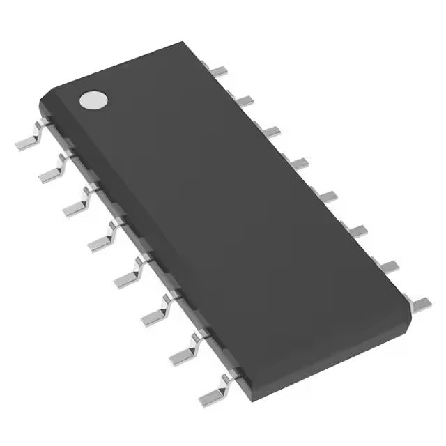
| Package Type | SOIC (16 pins) |
Key Features
- Buffered inputs
- Separate serial outputs synchronous to both positive and negative clock edges for cascading
- Fanout: Standard outputs support 10 LSTTL loads, bus driver outputs support 15 LSTTL loads
- Wide operating temperature range: −55°C to 125°C
- Balanced propagation delay and transition times
- Significant power reduction compared to LSTTL logic ICs
- HC types: 2- to 6-V operation, high noise immunity
- HCT types: 4.5- to 5.5-V operation, direct LSTTL input logic compatibility
- CMOS input compatibility with low input leakage current (Il ≤ 1 μA at VOL, VOH)
Applications
The CD74HCT4094M96 is suitable for a variety of applications where serial-to-parallel data conversion is necessary. These include:
- Digital display systems
- Serial data transmission systems
- Control and monitoring systems
- Automotive and industrial control systems
- Any application requiring high-speed serial shift registers with tri-state outputs
Q & A
- What is the operating voltage range of the CD74HCT4094M96?
The operating voltage range is 4.5 to 5.5 volts. - What is the maximum clock frequency for the CD74HCT4094M96?
The maximum clock frequency is 30 MHz. - How many stages does the shift register have?
The shift register has 8 stages. - What is the purpose of the Strobe input?
The Strobe input is used to transfer data from the shift register stage to the storage register. - Can the parallel outputs be connected directly to common bus lines?
Yes, the parallel outputs can be connected directly to common bus lines. - What is the fanout capability of the standard outputs?
The standard outputs can support up to 10 LSTTL loads. - What is the operating temperature range of the CD74HCT4094M96?
The operating temperature range is −55°C to 125°C. - How does the device handle cascading?
The device provides separate serial outputs synchronous to both positive and negative clock edges for cascading. - What is the input leakage current for CMOS inputs?
The input leakage current for CMOS inputs is less than or equal to 1 μA at VOL, VOH. - What package type is the CD74HCT4094M96 available in?
The CD74HCT4094M96 is available in a 16-pin SOIC package.


