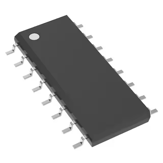
Overview
The CD74HC165MTE4 is a high-speed CMOS logic 8-bit parallel-in/serial-out shift register produced by Texas Instruments. This device is part of the HC165 series, which includes the CD54HC165, CD74HC165, CD54HCT165, and CD74HCT165. It is designed to operate in a wide range of temperatures and is suitable for various digital logic applications.
The device allows for both parallel and serial data loading, making it versatile for different system designs. When the parallel load (SH/LD) input is LOW, data from the A to H inputs is loaded into the register asynchronously. When the SH/LD is HIGH, data enters the register serially at the SER input and shifts one place to the right with each positive-going clock transition.
Key Specifications
| Parameter | Condition | Min | Max | Unit | |
|---|---|---|---|---|---|
| VCC Supply Voltage | - | -0.5 | - | 7 | V |
| Input Diode Current (VI < -0.5 V or VI > VCC + 0.5 V) | - | -20 | - | 20 | mA |
| Output Diode Current (VO < -0.5 V or VO > VCC + 0.5 V) | - | -20 | - | 20 | mA |
| Output Source or Sink Current per Output Pin | - | -25 | - | 25 | mA |
| Junction Temperature | - | - | - | 150 | °C |
| Storage Temperature | - | -65 | - | 150 | °C |
| Maximum Clock Pulse Frequency at VCC = 4.5V | - | - | 27 | - | MHz |
| Clock Pulse Width at VCC = 4.5V | - | 16 | 20 | 24 | ns |
| Set-up Time (SER to CLK) at VCC = 4.5V | - | 12 | 15 | 18 | ns |
Key Features
- Buffered inputs
- Asynchronous parallel load
- Complementary serial outputs (QH and Q H) available from the last stage
- Parallel-to-serial converter expansion capability by connecting the QH output to the SER input of the succeeding device
- High-speed CMOS logic
- Wide operating temperature range: -55°C to 125°C
- Available in various packages: SOIC, PDIP, and CERDIP
Applications
- Digital logic circuits requiring parallel-to-serial data conversion
- Microcontroller and microprocessor systems needing serial data transmission
- Communication systems, such as UARTs and serial interfaces
- Industrial control systems and automation
- Embedded systems and IoT devices
Q & A
- What is the primary function of the CD74HC165MTE4?
The primary function of the CD74HC165MTE4 is to act as an 8-bit parallel-in/serial-out shift register, allowing for both parallel and serial data loading.
- What are the operating temperature ranges for this device?
The device operates over a temperature range of -55°C to 125°C.
- What are the different package options available for the CD74HC165?
The device is available in SOIC, PDIP, and CERDIP packages.
- How does the parallel load feature work?
When the parallel load (SH/LD) input is LOW, data from the A to H inputs is loaded into the register asynchronously.
- What is the maximum clock pulse frequency at VCC = 4.5V?
The maximum clock pulse frequency at VCC = 4.5V is 27 MHz.
- What is the purpose of the complementary serial outputs (QH and Q H)?
The complementary serial outputs allow for easier integration into various digital circuits and enable parallel-to-serial converter expansion.
- How do you reset the shift register?
The shift register does not have a dedicated reset pin; however, the SH/LD input can be used to load new data asynchronously.
- What is the fanout capability of the device?
The device can drive up to 10 LSTTL loads over the temperature range.
- What are the typical applications of the CD74HC165MTE4?
Typical applications include digital logic circuits, microcontroller and microprocessor systems, communication systems, industrial control systems, and embedded systems.
- Is the CD74HC165MTE4 sensitive to electrostatic discharge?
Yes, the device is sensitive to electrostatic discharge, and users should follow proper IC handling procedures.


