


Overview
The CD74AC299M96 is a 3-state, 8-input universal shift/storage register with common parallel I/O pins, produced by Texas Instruments. This device utilizes advanced CMOS technology, offering high speed with significantly reduced power consumption compared to bipolar FAST/AS/S series. It features four synchronous-operating modes controlled by two select inputs, allowing for versatile use in various digital circuits. The register includes a master reset input and supports both serial and parallel data input/output operations.
Key Specifications
| Parameter | Value | Unit | Conditions |
|---|---|---|---|
| Supply Voltage (VCC) | 1.5 to 5.5 | V | |
| Propagation Delay (CP to Q0, Q7) | 3.1 to 12.9 | ns | VCC = 5V, TA = 25°C, CL = 50pF |
| Propagation Delay (CP to (I/O)n) | 3.6 to 14.5 | ns | VCC = 5V, TA = 25°C, CL = 50pF |
| Output Drive Current | ±24mA | mA | |
| Input Capacitance | 10 | pF | |
| 3-State Output Capacitance | 15 | pF | |
| Operating Temperature Range | -55 to +125°C | °C | Extended Industrial/Military |
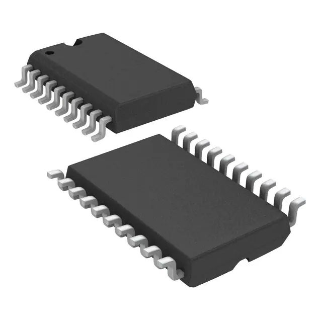
| Package Type | 20-lead SOIC (M suffix) |
Key Features
- SCR-Latchup-resistant CMOS process and circuit design: Ensures robust operation against latch-up conditions.
- High Speed with Low Power Consumption: Offers the speed of bipolar FAST/AS/S series with significantly reduced power consumption.
- Balanced Propagation Delays: Provides balanced noise immunity at 30% of the supply voltage.
- 3-State Input/Output Port: Supports three modes of operation - read, load, and disable I/O.
- Master Reset Input: Asynchronous active-LOW input for clearing the register.
- Cascadable: Can be expanded by cascading same units for larger storage needs.
Applications
The CD74AC299M96 is suitable for a variety of digital circuit applications, including:
- Shift Registers: For serial-to-parallel or parallel-to-serial data conversion.
- Storage Registers: For temporary data storage in digital systems.
- Counters and Timers: As part of more complex digital circuits requiring sequential data processing.
- Communication Systems: In serial data transmission and reception circuits.
- Microprocessor and Microcontroller Systems: For data buffering and storage.
Q & A
- What is the operating voltage range of the CD74AC299M96?
The operating voltage range is from 1.5V to 5.5V.
- What is the propagation delay for the CD74AC299M96?
The propagation delay from CP to Q0, Q7 is between 3.1ns and 12.9ns at VCC = 5V, TA = 25°C, and CL = 50pF.
- How much output drive current does the CD74AC299M96 provide?
The output drive current is ±24mA.
- What are the operating temperature ranges for the CD74AC299M96?
The device operates over the temperature ranges of 0 to 70°C (Commercial), -40 to +85°C (Industrial), and -55 to +125°C (Extended Industrial/Military).
- What is the package type for the CD74AC299M96?
The package type is a 20-lead SOIC (M suffix).
- Can the CD74AC299M96 be cascaded for larger storage needs?
- What is the function of the Master Reset input?
The Master Reset input is an asynchronous active-LOW input that clears the register regardless of the status of other inputs.
- How does the 3-state input/output port operate?
The 3-state input/output port supports three modes of operation: read, load, and disable I/O, controlled by the Output Enable inputs and Mode Select inputs.
- What are some common applications for the CD74AC299M96?
- What are the recommendations for power supply and layout?
The power supply should be bypassed with a 0.1μF capacitor, and layout guidelines include placing bypass capacitors near the positive supply terminal, using wide traces, and avoiding 90° corners for signal traces.


