


Overview
The CD4504BE-G, produced by Texas Instruments, is a CMOS Hex Voltage Level Shifter integrated circuit. This device consists of six circuits designed to shift input signals from one logic level to another, specifically from the VCC logic level to the VDD logic level. It is particularly useful for translating TTL signals to CMOS logic levels or between different CMOS levels. The CD4504BE-G is part of the CD4000 family and is available in various package types, including 16-lead dual-in-line plastic packages (DIP), small-outline packages (SOIC), and thin shrink small-outline packages (TSSOP).
Key Specifications
| Parameter | Value |
|---|---|
| Number of Channels | 6 |
| Technology | CMOS |
| Mounting Type | Through-Hole Technology (THT) |
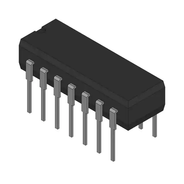
| Package Type | DIP16, SOIC, TSSOP |
| Operating Temperature Range | -55°C to 125°C |
| Input Voltage Range | 5V to 18V |
| Maximum Input Current | 1 µA at 18 V (full temperature range), 100 nA at 18 V and 25°C |
| Quiescent Current | 100% tested at 20 V |
Key Features
- Independence of power-supply sequence considerations: VCC can exceed VDD, and input signals can exceed both VCC and VDD.
- Up and down level-shifting capability.
- Shiftable input threshold for either CMOS or TTL compatibility.
- Standardized symmetrical output characteristics.
- Low maximum input current: 1 µA at 18 V over the full package-temperature range, and 100 nA at 18 V and 25°C.
- Compliance with JEDEC Standard No. 13B for B Series CMOS Devices.
Applications
The CD4504BE-G is versatile and can be used in various applications where level shifting between different logic levels is necessary. Some common applications include:
- Translating TTL signals to CMOS logic levels.
- Translating signals between different CMOS logic levels.
- Use in digital circuits requiring level shifting, such as in microcontroller or microprocessor systems.
- Integration in mixed-signal designs where different voltage levels are used.
Q & A
- What is the primary function of the CD4504BE-G?
The primary function of the CD4504BE-G is to shift input signals from one logic level to another, specifically from the VCC logic level to the VDD logic level.
- What types of logic levels can the CD4504BE-G handle?
The CD4504BE-G can handle both TTL and CMOS logic levels and can translate between them or between different CMOS levels.
- What are the available package types for the CD4504BE-G?
The CD4504BE-G is available in 16-lead dual-in-line plastic packages (DIP), small-outline packages (SOIC), and thin shrink small-outline packages (TSSOP).
- What is the operating temperature range of the CD4504BE-G?
The operating temperature range of the CD4504BE-G is -55°C to 125°C.
- What is the maximum input current of the CD4504BE-G?
The maximum input current is 1 µA at 18 V over the full package-temperature range, and 100 nA at 18 V and 25°C.
- Is the CD4504BE-G RoHS compliant?
- What is the significance of the SELECT input in the CD4504BE-G?
The SELECT input determines whether the device translates TTL signals to CMOS logic levels (SELECT at VCC HIGH) or translates signals between different CMOS levels (SELECT at LOW).
- Can the CD4504BE-G operate with different power supply sequences?
- Is the CD4504BE-G still in production?
- What standards does the CD4504BE-G comply with?


