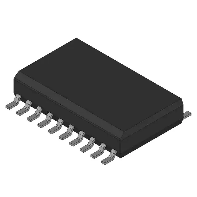
Overview
The 74LS323SCX is an 8-bit universal shift/storage register with 3-state outputs, manufactured by National Semiconductor. This component is designed for applications requiring data storage and shifting operations, making it a versatile choice for digital systems. Its market positioning targets engineers and developers working on bus-oriented applications, such as data processing and communication systems. The 74LS323SCX stands out for its synchronous reset functionality and multiplexed parallel load inputs, which minimize pin count and simplify circuit design.
Key Specifications
| Parameter | Value | Unit | Notes |
|---|---|---|---|
| Number of Bits | 8 | - | Universal shift/storage register |
| Output Type | 3-state | - | Bus-oriented applications |
| Operation Modes | Shift Left, Shift Right, Parallel Load, Hold | - | Activated on LOW-to-HIGH clock transition |
| Clock Frequency | Up to 25 MHz | MHz | Typical operating condition |
| Supply Voltage | 4.75 to 5.25 | V | Standard TTL levels |
| Power Dissipation | 100 | mW | Maximum value |
Key Features
- Multiplexed Parallel Load Inputs: Reduces pin count and simplifies circuit design.
- Synchronous Reset: Ensures precise control over register operations.
- 3-State Outputs: Enables bus-oriented applications with high impedance states.
- Four Operation Modes: Supports shift left, shift right, parallel load, and hold functions.
- Separate I/O for Cascading: Facilitates easy expansion for larger data handling needs.
Applications
The 74LS323SCX is widely used in digital systems requiring data storage and shifting capabilities. Its primary applications include:
- Data Processing Systems: For temporary storage and manipulation of data.
- Communication Systems: For serial-to-parallel or parallel-to-serial data conversion.
- Bus-Oriented Systems: For interfacing multiple devices on a shared bus.
- Industrial Automation: For control and monitoring of digital signals.
Q & A
1. What is the primary function of the 74LS323SCX?
The 74LS323SCX is an 8-bit universal shift/storage register designed for data storage and shifting operations in digital systems.
2. What are the key operation modes of this component?
It supports four operation modes: shift left, shift right, parallel load, and hold.
3. How does the synchronous reset feature work?
The synchronous reset ensures that the register is reset precisely on the LOW-to-HIGH transition of the clock signal.
4. What is the significance of 3-state outputs?
3-state outputs allow the device to enter a high impedance state, making it suitable for bus-oriented applications.
5. What is the maximum clock frequency supported?
The 74LS323SCX can operate at clock frequencies of up to 25 MHz.
6. What is the supply voltage range for this component?
It operates within a supply voltage range of 4.75 to 5.25 volts.
7. Can the 74LS323SCX be cascaded for larger data handling?
Yes, separate I/O pins for Q0 and Q7 enable easy cascading of multiple devices.
8. What are typical applications of this component?
Typical applications include data processing, communication systems, bus-oriented systems, and industrial automation.
9. What is the power dissipation of the 74LS323SCX?
The maximum power dissipation is 100 mW.
10. How does the multiplexed parallel load feature benefit circuit design?
This feature minimizes pin count and simplifies circuit design by combining parallel load inputs with flip-flop outputs.


