


Overview
The MC74LV594ADR2G, produced by onsemi, is an 8-bit shift register with an integrated output register. This device is designed to operate over a wide voltage range of 2.0 V to 6.0 V, making it versatile for various applications. It features an 8-bit serial-in, parallel-out shift register that feeds an 8-bit D-type storage register. The device includes separate clocks for the shift and storage registers (RCLK and SRCLK) and direct overriding clear inputs (RCLR and SRCLR) for each register. This component is particularly useful in systems requiring sequential data processing and storage.
Key Specifications
| Parameter | Min | Typ | Max | Unit |
|---|---|---|---|---|
| VCC (DC Supply Voltage) | 2.0 | 6.0 | V | |
| VI (DC Input Voltage) | 0 | VCC + 0.5 | V | |
| VO (DC Output Voltage Active Mode) | 0 | VCC + 0.5 | V | |
| TA (Operating Free-Air Temperature) | -55 | 85 | °C | |
| tPD (Propagation Delay Low to High) | 18 | 22.5 | 27.5 | ns (at VCC = 3.0 V to 3.6 V) |
| fMAX (Maximum Clock Frequency) | 65 | 80 | MHz (at CL = 15 pF, VCC = 2.3 V to 2.7 V) | |
| ICC (DC Supply Current per Supply Pin) | 8.0 | 80 | μA (at VCC = 6.0 V) | |
| CI (Input Capacitance) | 3.3 | 3.5 | pF |
Key Features
- 2.0 V to 6.0 V VCC operation
- Low input current: 1.0 μA
- Maximum propagation delay (tpd) of 6.5 ns at 5 V
- Typical VOLP (Output Ground Bounce) < 0.8 V at VCC = 3.3 V, TA = 25°C
- Typical VOHV (Output VOH Undershoot) > 2.3 V at VCC = 3.3 V, TA = 25°C
- Support for mixed-mode voltage operation on all ports
- 8-bit serial-in, parallel-out shift registers with storage
- Independent direct overriding clears on shift and storage registers
- Independent clocks for shift and storage registers
- High noise immunity characteristic of CMOS devices
- In compliance with the requirements defined by JEDEC Standard No. 7A
- Pb-free, halogen-free/BFR-free, and RoHS compliant
Applications
The MC74LV594ADR2G is suitable for a variety of applications, including:
- Sequential data processing and storage in digital systems
- Cascading shift registers for extended data lengths
- Display drivers and LED drivers requiring serial-to-parallel conversion
- Industrial control systems and automation
- Consumer electronics requiring low power and high noise immunity
Q & A
- What is the operating voltage range of the MC74LV594ADR2G?
The MC74LV594ADR2G operates over a voltage range of 2.0 V to 6.0 V.
- What type of shift register does the MC74LV594ADR2G contain?
The device contains an 8-bit serial-in, parallel-out shift register.
- What are the maximum propagation delays for the MC74LV594ADR2G?
The maximum propagation delay is 6.5 ns at 5 V.
- Does the MC74LV594ADR2G support mixed-mode voltage operation?
- What are the independent clock inputs for the shift and storage registers?
The independent clock inputs are RCLK for the storage register and SRCLK for the shift register.
- Is the MC74LV594ADR2G RoHS compliant?
- What is the maximum clock frequency for the MC74LV594ADR2G?
The maximum clock frequency is 65 MHz at CL = 15 pF and VCC = 2.3 V to 2.7 V.
- How many bits does the shift register in the MC74LV594ADR2G have?
The shift register has 8 bits.
- What are the package options available for the MC74LV594ADR2G?
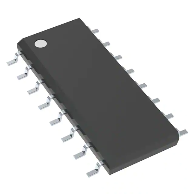
The device is available in SOIC-16 and TSSOP-16 packages.
- What is the thermal resistance of the SOIC package for the MC74LV594ADR2G?
The thermal resistance for the SOIC package is 112 °C/W.


