


Overview
The HEF4094BTT-Q100118 is an 8-bit serial-in/serial or parallel-out shift register with a storage register and 3-state outputs, manufactured by NXP USA Inc. This device is part of the HEF4000 family and is qualified to the Automotive Electronics Council (AEC) standard Q100 (Grade 1), making it suitable for automotive applications. It features separate clocks for both the shift and storage registers, enabling flexible data handling and cascading capabilities.
Key Specifications
| Type number | VCC (V) | Logic switching levels | Output drive capability (mA) | tpd (ns) | fmax (MHz) | Number of bits | Power dissipation considerations | Tamb (°C) | Rth(j-a) (K/W) | Ψth(j-top) (K/W) | Rth(j-c) (K/W) | Package name |
|---|---|---|---|---|---|---|---|---|---|---|---|---|
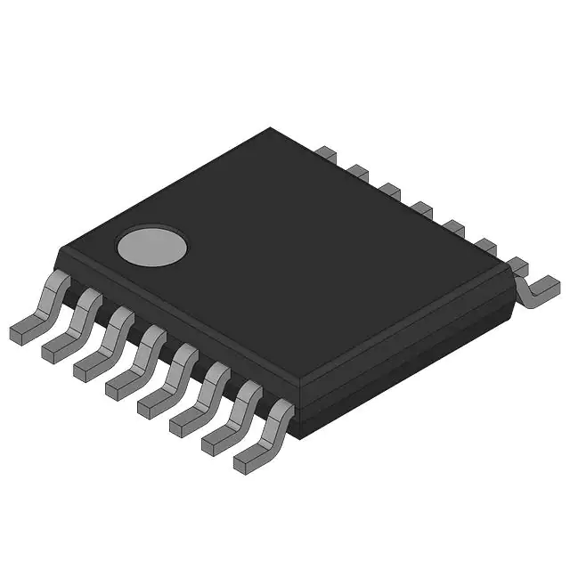
| HEF4094BTT-Q100118 | 3.0 - 15 | CMOS | ± 2.4 | 50 | 28 | 8 | medium | -40 to +85, -40 to +125 | 121 | 3.8 | 50.9 | TSSOP16 |
Key Features
- 8-bit serial-in/serial or parallel-out shift register with a storage register and 3-state outputs.
- Separate clocks for the shift and storage registers.
- Serial input (D) and two serial outputs (QS1 and QS2) for cascading.
- Data shifted on LOW-to-HIGH transitions of the CP input.
- Data transfer from shift register to storage register when STR input is HIGH.
- Output enable input (OE) controls output state without affecting register state.
- Inputs include clamp diodes for interfacing with voltages in excess of VDD.
- Fully static operation.
- Wide supply voltage range from 3.0 V to 15.0 V.
- CMOS low power dissipation.
- High noise immunity.
- Standardized symmetrical output characteristics.
- Complies with JEDEC standard JESD 13-B.
- ESD protection: HBM exceeds 2000 V, CDM exceeds 1000 V.
Applications
The HEF4094BTT-Q100118 is suitable for various applications, including:
- Automotive systems due to its AEC-Q100 (Grade 1) qualification.
- Industrial control systems requiring serial-to-parallel data conversion.
- Communication systems needing data buffering and shifting.
- Consumer electronics where low power consumption and high noise immunity are crucial.
Q & A
- What is the primary function of the HEF4094BTT-Q100118?
The primary function is to act as an 8-bit serial-in/serial or parallel-out shift register with a storage register and 3-state outputs.
- What is the supply voltage range for this device?
The supply voltage range is from 3.0 V to 15.0 V.
- How does the device handle data transfer between the shift and storage registers?
Data is transferred from the shift register to the storage register when the STR input is HIGH.
- What is the significance of the OE input?
The OE input controls the output state, setting it to a high-impedance OFF-state when LOW, without affecting the state of the registers.
- What kind of ESD protection does the device offer?
The device offers ESD protection exceeding 2000 V for HBM and 1000 V for CDM.
- What is the operating temperature range for this device?
The device operates from -40 °C to +85 °C and -40 °C to +125 °C.
- What package type is used for the HEF4094BTT-Q100118?
The device is packaged in a TSSOP16 (SOT403-1).
- Is the device suitable for automotive applications?
Yes, it is qualified to the Automotive Electronics Council (AEC) standard Q100 (Grade 1).
- What are the key benefits of using CMOS technology in this device?
CMOS technology provides low power dissipation and high noise immunity.
- How does the device support cascading?
The device supports cascading through two serial outputs (QS1 and QS2) and allows data to be available on different clock edges.


