


Overview
The 74HCT595PW-Q100118 is an 8-bit serial-in/serial or parallel-out shift register produced by NXP USA Inc. (now part of Nexperia). This component features a storage register and 3-state outputs, making it versatile for various digital circuit applications. It is qualified to the Automotive Electronics Council (AEC) standard Q100 (Grade 1), ensuring its reliability in automotive and other demanding environments.
Key Specifications
| Type number | VCC (V) | Logic switching levels | Output drive capability (mA) | tpd (ns) | fmax (MHz) | Number of bits | Power dissipation considerations | Tamb (°C) | Rth(j-a) (K/W) | Ψth(j-top) (K/W) | Rth(j-c) (K/W) | Package name |
|---|---|---|---|---|---|---|---|---|---|---|---|---|
| 74HCT595PW-Q100 | 4.5 - 5.5 | TTL | ± 6 | 25 | 57 | 8 | Low | -40 to +125 | 123 | 4.1 | 52.2 | TSSOP16 |
Key Features
- 8-bit serial-in, serial or parallel-out shift register with output latches and 3-state outputs.
- Separate clocks for shift and storage registers.
- Serial input (DS) and serial output (Q7S) for cascading.
- Asynchronous reset MR input; a LOW on MR resets the shift register.
- Data shifted on LOW-to-HIGH transitions of the SHCP input.
- Data transferred to the storage register on LOW-to-HIGH transition of the STCP input.
- Output enable input (OE) controls output state; HIGH on OE sets outputs to high-impedance OFF-state.
- Inputs include clamp diodes for voltage protection.
- ESD protection: HBM exceeds 2000 V, CDM exceeds 1000 V.
- Typical shift out frequency of 100 MHz.
- Automotive product qualification in accordance with AEC-Q100 (Grade 1).
Applications
- Serial-to-parallel data conversion.
- Remote control holding register.
- Automotive applications due to AEC-Q100 qualification.
- General digital circuitry requiring shift register functionality.
Q & A
- What is the primary function of the 74HCT595PW-Q100118?
The primary function is to act as an 8-bit serial-in/serial or parallel-out shift register with a storage register and 3-state outputs.
- What are the logic switching levels for the 74HCT595PW-Q100118?
The logic switching levels are TTL (Transistor-Transistor Logic).
- How is data shifted in the shift register?
Data is shifted on the LOW-to-HIGH transitions of the SHCP input.
- What is the effect of the OE input on the outputs?
A HIGH on the OE input causes the outputs to assume a high-impedance OFF-state.
- What is the typical shift out frequency of the 74HCT595PW-Q100118?
The typical shift out frequency is 100 MHz.
- Does the 74HCT595PW-Q100118 have ESD protection?
- What is the operating temperature range for the 74HCT595PW-Q100118?
The operating temperature range is from -40 °C to +125 °C.
- What package options are available for the 74HCT595PW-Q100118?
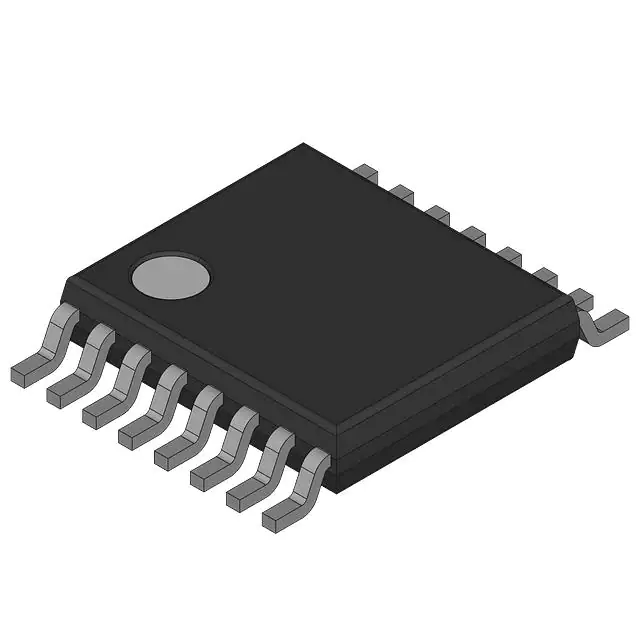
It is available in TSSOP16 package.
- Is the 74HCT595PW-Q100118 qualified for automotive applications?
- Can the 74HCT595PW-Q100118 be cascaded?
- How does the asynchronous reset MR input work?
A LOW on the MR input resets the shift register.


